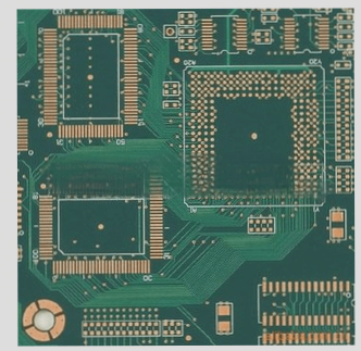
Evolution of PCB Production and Via Hole Plugging Technology
The production process for printed circuit boards (PCBs) and surface mount technology has advanced to meet increasing demands. Via hole plugging technology has emerged to address these needs, with specific requirements:
- The via holes in the PCB must contain copper, with the option for plugging or leaving the solder mask unplugged.
- Via holes must have a tin and lead layer of at least 4 microns thickness, with no solder mask ink entering to avoid hidden tin beads.
- Through holes should be plugged with opaque solder mask ink, ensuring no tin rings or beads are present and meeting flatness standards.
As electronic products become smaller and more complex, PCBs have followed suit, leading to the popularity of surface mount technology (SMT) and ball grid array (BGA) PCBs. Customers now require via hole plugging during component mounting for various functions:
- Preventing tin flow through the component surface via the hole during wave soldering, crucial for BGA pad placements.
- Avoiding flux residue accumulation in via holes.
- After component assembly, the PCB undergoes vacuum processing for final testing completion.
- Preventing surface solder paste from flowing into holes, which could cause false soldering.
- Preventing solder balls from causing short circuits during wave soldering.
Conductive Hole Plugging Process Implementation
For surface mount boards, especially those with BGA and IC components, via hole plugging must be uniform with no deviations. The process flow can vary significantly, with challenges in process control. Different PCB plugging processes are summarized below, with comparisons of their advantages and disadvantages.
Hole Plugging Process After Hot Air Leveling
The process involves board surface solder mask → HAL → plug hole → curing. Plugging ink can be photosensitive or thermosetting. Consistent ink usage for via hole plugging and board surface is ideal to prevent solder loss. However, contamination risks and potential false soldering, especially in BGA placements, are drawbacks.
Hot Air Leveling and Plug Hole Technology
Using Aluminum Sheets for Hole Plugging, Curing, and Grinding
A CNC drilling machine creates an aluminum sheet screen to fill via holes, using durable, low-resin shrinkage, and adhesive thermosetting ink. The process flow includes pre-treatment → plug hole → grinding → pattern transfer → etching → board surface solder mask.
Methods for Via Hole Plugging in PCB Manufacturing
1. Copper Wall Thickening for Via Hole Plugging
To ensure flat and high-quality via hole plugging, a one-time copper thickening step is required before hot air leveling. This step is essential to meet customer specifications for copper wall thickness. However, some PCB factories lack the necessary equipment for this process, limiting its widespread use.
2. Aluminum Sheet Plugging, Screen Printing, and Solder Mask Application
This method involves using a CNC drilling machine to create an aluminum sheet screen for hole plugging. The process flow includes pre-treatment, hole plugging, screen printing, pre-baking, exposure, development, and curing. It ensures good coverage of via holes with solder mask, preventing issues like tinning or hidden solder balls post hot air leveling. However, post-curing challenges may lead to solderability issues and solder mask loss.
3. Aluminum Sheet Plugging, Development, Pre-Curing, and Soldering After Grinding
Here, a CNC drilling machine is used to create an aluminum sheet for plugging, followed by installation on a screen printing machine. The process flow includes pre-treatment, hole plugging, pre-baking, development, pre-curing, and solder mask application. While this method maintains solder mask coverage, it may not fully address tin ball concerns in via holes.
4. Simultaneous Board Surface Solder Mask and Plug Hole Application
This approach involves using a screen printer with a 36T (43T) screen to simultaneously plug board surface and via holes. The process flow consists of pre-treatment, screen printing, pre-baking, exposure, development, and curing. While offering efficiency and maintaining solder mask integrity, issues like solder mask breakage during curing and hidden vias post hot air leveling may still occur.
If you require PCB manufacturing services, feel free to contact us.