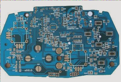
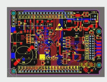
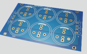
There are single-sided, double-sided, and multi-layer PCB boards, with multi-layer boards having no limit to their number—some exceeding 100 layers. Common configurations include four-layer and six-layer boards. So, why do we observe that “multi-layer PCBs” tend to have even-numbered layers? Generally, even-numbered PCBs are indeed more prevalent than their odd-numbered counterparts and offer certain advantages.

01Lower Cost

Due to the absence of an additional layer of dielectric and foil, the raw material costs for odd-numbered PCBs are slightly lower than those for even-numbered ones. However, the processing costs for odd-layer PCBs are significantly higher than for even-layer boards. While the inner layer processing costs remain the same, the foil/core structure notably elevates the processing costs of the outer layer. Odd-numbered PCBs require a non-standard laminated core layer bonding process, which complicates production. In contrast, factories that incorporate foil into the core structure experience a decline in production efficiency.

Before lamination and bonding, the outer core undergoes additional processing, heightening the risk of scratches and etch errors on the outer layer.

02Balanced structure prevents bending

The primary reason to avoid designing a PCB with an odd number of layers is that such boards are prone to bending. After the multilayer circuit bonding process, varying lamination tensions in the core and foil-clad structures can cause bending during cooling. As the circuit board’s thickness increases, the likelihood of bending in a composite PCB with differing structures also rises. The solution to mitigating circuit board bending lies in employing a balanced stack. While a PCB exhibiting some bending may meet specifications, it can reduce processing efficiency and elevate costs, as specialized equipment and techniques are needed during assembly, compromising component placement accuracy and overall quality.

To clarify: in PCB fabrication, four-layer boards offer better control than three-layer boards, particularly in terms of symmetry. The warpage of a four-layer board can be maintained below 0.7% (IPC600 standard). In contrast, larger three-layer boards often exceed this standard, adversely affecting SMT patch reliability and overall product integrity. Consequently, designers typically avoid odd-numbered layer boards; if functions necessitate it, they may design a “faux” even-numbered layer, converting 5 layers into 6, or 7 layers into 8.

Given these considerations, most multilayer PCBs are designed with even numbers of layers, with fewer odd-numbered designs.

03How to achieve balanced stacking and reduce costs for odd-numbered PCBs?

What if an odd-numbered PCB arises in the design? The following methods can promote balanced stacking, lower manufacturing costs, and prevent PCB bending.

1) Utilize a signal layer. This approach is applicable when the power layer is even, and the signal layer is odd. Adding this layer incurs no extra costs, while also shortening delivery times and enhancing PCB quality.

2) Incorporate an additional power layer. This method is suitable when the power layer is odd, and the signal layer is even. Simply insert a layer in the middle of the stack without altering other configurations. First, route the traces in the odd-numbered layer PCB, then duplicate the ground layer in the middle, and label the remaining layers. This achieves electrical characteristics similar to those of a thickened foil layer.

3) Introduce a blank signal layer near the center of the PCB stack. This strategy minimizes stacking imbalance and enhances PCB quality. First, route according to the odd-numbered layers, then add a blank signal layer, labeling the remaining layers. This approach is effective for microwave circuits and mixed media circuits with varying dielectric constants.


Let me know if you need further adjustments!

Leave a Comment

Contact

WellCircuits
More than PCB

Upload your GerberFile(7z,rar,zip)