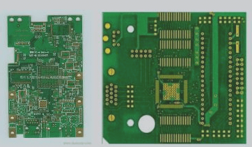
PCB Secondary Design and Development
Introduction to PCB Secondary Design and Development
When delving into PCB secondary design and development, it’s crucial to integrate the latest advanced technologies to enhance product functionality and reduce costs. The challenge lies in effectively incorporating these cutting-edge technologies into the design.
Factors to Consider in PCB Design
During the process, numerous factors must be taken into account, with time to market being one of the most critical. Decisions around this factor can evolve continuously, considering product functionality, design feasibility, testing requirements, and ensuring EMI compliance.
Impact of Previous Work on Design Efficiency
The quality and completeness of prior work play a significant role in minimizing design iteration. Identifying and resolving issues in the early stages is easier, while addressing problems in later phases can be more challenging and costly.
The Role of Integrated Design Software
High-quality integrated design software is essential in PCB design, yet the high cost often limits accessibility. While advanced software can streamline the design process, the price point may pose constraints for some companies.
Evaluating PCB Design Tools
This article explores the challenges in PCB secondary design and highlights key factors to consider when selecting a PCB design tool. Understanding these factors is crucial for PCB designers to choose software that balances functionality, cost, and design efficiency.

Factors for PCB Designers to Consider:
- Product Function
- The basic functional requirements of the product, including:
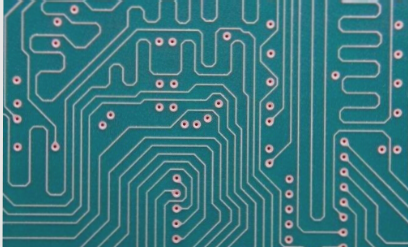
- Interaction between schematic design and PCB layout
- Wiring capabilities adhering to design rule constraints
- Accurate DRC (Design Rule Check) functionality
- The basic functional requirements of the product, including:
- Choosing a Strong Technical Partner
- A reliable partner with industry-leading expertise can help design products efficiently with cutting-edge technology.
- Price Considerations
- Price is crucial, but the focus should be on the return on investment.
When selecting PCB design tools, designers must evaluate various factors based on the complexity of the design tasks. As systems become more intricate, controlling physical routing and component placement becomes crucial, requiring the establishment of constraints. However, imposing too many constraints can limit design flexibility. Designers need a deep understanding of their design requirements and rules to apply them appropriately.