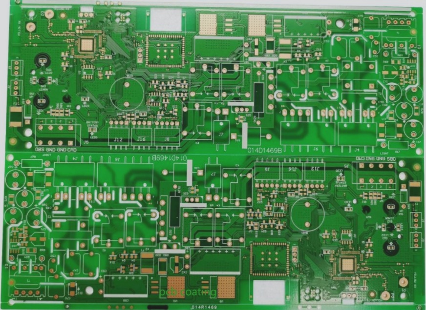
There are several reasons for general copper plating.
First, one of the advantages of copper plating is to reduce the impedance of the ground wire (a large part of the so-called anti-interference is also caused by the reduction of the impedance of the ground wire). There are a large number of spike currents in the digital circuit, so it is more necessary to reduce the impedance of the ground wire. It is generally believed that for circuits composed of digital devices, a large area should be laid, while for analog circuits, the ground loop formed by laying copper will cause electromagnetic coupling interference (except for high-frequency circuits). Therefore, not all circuits need to be made of copper (BTW: mesh copper is better than the whole block).
Second, the significance of copper circuit:
Third, what is the difference between a copper-clad block and a grid? Specifically, there are about 3 functions: 1. Beautiful appearance 2. Noise suppression 3. In order to reduce high-frequency interference (for the reason on the circuit board), according to the wiring guidelines: the power supply and the ground floor should be as wide as possible, why should we add grids Ah, isn’t it inconsistent with the principle? If you look at it from a high frequency point of view, it is even more wrong. The most taboo thing in high frequency wiring is sharp traces. There are many problems in the power layer with more than 90 degrees. In fact, why it is done that way is entirely a requirement of the craftsmanship: see if the hand-soldered ones are painted like that, almost none; if you see such paintings, there must be a post chip on it, because there is a process during the patch. It is called wave soldering. It needs to locally heat the board. If the specific heat coefficients of the two sides are different, the board will be tilted up, and the problem will come when the board is tilted. It is easy to make mistakes and the rejection rate goes straight up. In fact, this approach also has disadvantages: under our current corrosion process: the film is easy to stick to it. In the following strong acid project, that point may not corrode, and there are many waste products, but only if the board is broken and the chip on it is finished with the board!
Some surface mounts do not have grids. From the perspective of product consistency, there may be two situations: 1. His corrosion process is very good; 2. It does not use wave soldering but uses more advanced reflow soldering, but in this case, the investment of the entire assembly line will go up 3-5 times.


