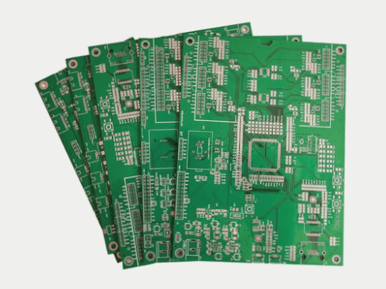
PCB Board Layout and EMI Control Strategies
This article delves into the intricacies of PCB board layout and the critical role of PCB layer stacking in managing EMI emissions.
1. Power Bus Optimization
- Strategic placement of capacitors near IC power pins can enhance output voltage stability.
- Power plane design surrounding the IC acts as a high-frequency capacitor, reducing common-mode EMI interference.
- Minimizing power supply layer inductance is vital for EMI reduction.
2. Electromagnetic Shielding Techniques
- Effective layering involves positioning signal traces adjacent to power or ground planes.
- Proximity of power and ground layers, known as the “layering” strategy, aids in EMI control.
3. Advanced PCB Stacking Methods
Explore various stacking strategies to shield and suppress EMI emissions.
4. Enhanced 4-Layer Board Design
Consider innovative designs with ground layers on the outer sides and signal/power layers in the middle for improved EMI suppression.
5. Benefits of a 6-Layer Board
For high component density situations, a 6-layer board can help in reducing transient signals and electromagnetic field interference.
6. Signal Integrity in 10-Layer Boards
Ensure optimal signal paths by allocating layers for signal lines adjacent to ground layers in 10-layer boards.
7. Designing Multiple Power Layers
Implement separate power and ground planes with insulation layers for uniform current distribution and minimized EMI in high-current scenarios.
8. Conclusion
Effective layer stacking is crucial for bypassing power buses, decoupling signals, and shielding electromagnetic fields in PCB designs. Adhering to fundamental principles ensures successful EMI management in the face of evolving technological challenges.


