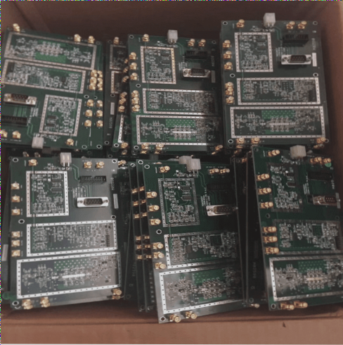
The Importance of SM Placement Process in PCB Production
Overview of SMT Patch Processing
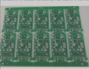
- Material Procurement, Processing, and Inspection
- Silk Screen Printing
- Dispensing
- Mounting
- Curing
- Reflow Soldering
- Cleaning
- Detection
- Repair
Material procurement is initiated based on the customer’s BOM list to ensure production accuracy. Materials undergo inspection and processing, including tasks like pin header cutting and resistor pin forming. Nuo’s electronic material procurement is handled by specialized suppliers for comprehensive processes.
Silk screen printing is the initial step in SMT processing, where solder paste or adhesive is applied to PCB pads for component soldering. The thickness of the solder paste application is crucial for PCB processing requirements.
Adhesive, typically red glue, is dispensed on specific PCB positions to secure components during soldering, preventing dislodging during reflow soldering.
The placement machine positions SMC/SMD components accurately on designated pads without damage, utilizing suction and placement functions.
Heat curing melts the adhesive to secure surface mount components onto PCB pads.
Reflow soldering establishes connections between solder joints of components and PCB pads using hot air flow.
After soldering, the PCB surface is cleaned to remove flux residues and solder balls that can cause short circuits.
Inspection techniques like AOI optical inspection and function testing are crucial for assessing welding and assembly quality.
SMT repair involves removing non-functional components and repairing damaged parts to ensure PCB functionality.
Latest Update: Innovations in SMT Patch Processing
Recent advancements in SMT patch processing include the integration of AI for automated inspection, enhancing quality control and efficiency in PCB production. Additionally, the use of environmentally friendly solder pastes has become a focus to reduce ecological impact.
Looking Ahead: Future Trends in SM Placement
The future of SM placement in PCB production is moving towards miniaturization and increased automation. Technologies such as 3D printing for customized solder stencils and machine learning for predictive maintenance are poised to revolutionize the industry.
Need Further Adjustments?
Don’t hesitate to reach out if you require any additional modifications!