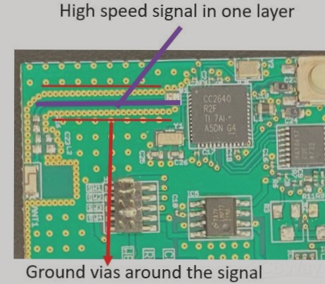
**PCB Copy Board**, often referred to in the industry as circuit board copying, circuit board cloning, PCB cloning, PCB reverse design, or PCB reverse development, involves the process of reverse engineering a circuit board. This process is based on the physical presence of the electronic product and its associated circuit board. Using reverse R&D techniques, engineers perform an in-depth analysis of the circuit board. The goal is to reconstruct the original PCB design files, Bill of Materials (BOM), schematic diagrams, and other essential technical documents, as well as PCB silkscreen production files. These documents are then used to manufacture the PCB, solder components, perform flying probe testing, debug the circuit board, and essentially replicate the original PCB template.

1. **Reasonably Divide Functional Areas**

When conducting reverse design on the schematic of a well-designed PCB, a thoughtful division of functional areas can greatly assist engineers in avoiding unnecessary complications and enhance drawing efficiency. In general, components with similar functions on a PCB are grouped together in close proximity. This functional area division serves as a clear and effective basis when reconstructing the schematic diagram, ensuring both precision and convenience during the reverse engineering process.


1. **Understanding the Division of Functional Areas**

The division of functional areas is not arbitrary; it requires engineers to have a solid understanding of electronic circuit principles. First, identify the core component within a given functional unit. Then, based on the wiring connections, trace other components of the same unit, forming a complete functional partition. This process is the foundation for creating a schematic diagram. Additionally, don’t forget to leverage the component serial numbers on the PCB. These can significantly expedite the functional partitioning process.

2. **Select Appropriate Reference Components**

Reference components, also known as the main parts in the PCB layout during the schematic design, play a critical role. Once the reference components are identified, the schematic can be drawn based on the pins of these components, ensuring greater accuracy. For engineers, selecting reference components is not overly complex. Typically, the key components in the circuit—those that are larger in size and have more pins—serve as the most suitable reference parts. Examples include integrated circuits, transformers, and transistors, among others.

3. **Correctly Identify and Route Wiring**

Distinguishing between ground, power, and signal lines requires a good understanding of power supply design, circuit connections, and PCB routing techniques. These lines can be differentiated by factors such as component connections, trace width, and the specific requirements of the electronic product. To avoid trace overlap, it’s helpful to use grounding symbols for the ground traces. Different colors and line types can be used for various lines to ensure clarity and ease of identification. For individual components, specialized symbols or even separate unit circuit drawings can be employed, which are later combined.

4. **Understand the Basic Framework and Learn from Similar Schematics**

Engineers need to be well-versed in the basic structure of electronic circuits and schematic diagramming techniques. This includes being able to directly draw simple, classic unit circuits and organizing the overall layout of electronic circuits. Additionally, it’s important to recognize that similar types of electronic products tend to have similar schematic layouts. Engineers should leverage their experience and learn from existing circuit diagrams to help design schematics for new products.

5. **Verification and Optimization**

Once the schematic is complete, the reverse engineering of the PCB schematic can be considered done after testing and validation. Special attention should be given to components that are sensitive to the PCB’s distribution parameters, ensuring their nominal values are correct. The schematic should be compared and analyzed against the PCB file diagram to confirm that they match perfectly.

These are the key points to consider when reverse-engineering a PCB schematic diagram.

Leave a Comment

Contact

WellCircuits
More than PCB

Upload your GerberFile(7z,rar,zip)