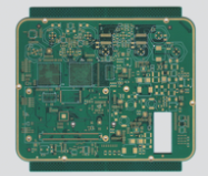
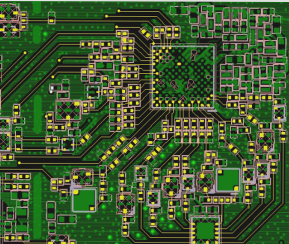
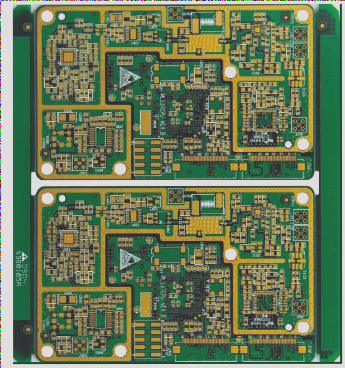
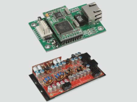
The technical process of PCB cloning involves scanning the circuit board to be copied, documenting the precise component locations, and then removing the components to create the Bill of Materials (BOM). Following this, material procurement is arranged, and the empty PCB is scanned, processed using PCB cloning software, and converted into a PCB layout file. The PCB file is then sent to the fabrication plant to manufacture the board. After the board is produced, the components are soldered onto the newly created PCB, and the circuit board is tested and debugged.
Specific Steps for PCB Cloning:
1. Start with a PCB, and first document the model, parameters, and placement of all essential components, paying particular attention to the orientation of diodes, transistors, and the pin 1 indicator of ICs. It’s best to take two photographs of the critical component locations using a digital camera. Modern PCB cloning techniques are becoming more sophisticated, and some diodes and transistors may be overlooked if not inspected closely.
2. Remove any multi-layer boards and components, and desolder the pads (remove solder from the PAD holes). Clean the PCB with alcohol, then place it into the scanner. When scanning, increase the resolution slightly for a clearer image. Afterward, gently polish the top and bottom layers with a fine abrasive cloth until the copper surface is shiny. Put the cleaned PCB into the scanner, open Photoshop, and scan both layers in color separately. Ensure that the PCB is aligned both horizontally and vertically in the scanner; otherwise, the scan may be unusable.
3. Adjust the contrast and brightness of the scanned images to create a sharp contrast between the copper areas and the non-copper areas. Convert the second image to black and white and verify that the lines are clearly visible. If not, repeat the process. Once the image is clear, save it in BMP format as TOP.BMP and BOT.BMP. If there are any discrepancies or imperfections in the image, use Photoshop to correct them.
4. Convert the two BMP files to PROTEL format and import them into two separate layers in PROTEL. Ensure that the positions of pads (PAD) and vias on the two layers align correctly. If they do not, revisit Step 3. PCB cloning requires precision and patience—small errors can compromise the final outcome and alignment.
5. Convert the BMP file of the TOP layer into a TOP.PCB file, ensuring you correctly map the SILK layer (the yellow layer). Afterward, trace the lines on the TOP layer and place the components according to the layout created in Step 2. Once completed, delete the SILK layer. Repeat this process for all layers until the entire design is traced.
6. Import the TOP.PCB and BOT.PCB files into PROTEL and combine them into a single layout. If everything is correctly aligned, this will complete the PCB design.
7. Finally, print the TOP and BOTTOM layers onto transparent film using a laser printer, ensuring a 1:1 ratio. Place the film over the cloned PCB and verify that the layers align correctly. If everything matches, the PCB cloning process is complete.

A copy of the original board has been created, but this is only part of the process. It is also necessary to test whether the electronic performance of the copy board matches that of the original. If the performance is identical, then the job is truly complete.
**Note:** For multilayer boards, special care must be taken when polishing the inner layers. The copying steps (from step 3 to step 5) should be repeated. Of course, the naming of the layers also differs depending on the number of layers involved. Generally, double-sided boards are much easier to copy than multilayer boards. Multilayer copies are more prone to misalignment, so extra caution is needed, especially when dealing with internal vias and non-vias.
### Double-Sided Copy Board Method:
1. Scan the top and bottom layers of the circuit board and save each as a BMP image.
2. Open the copy board software Quickpcb2005, click “File” and select “Open Base Map” to load the scanned image. Use the PAGEUP key to zoom in and view the pads. Press PP to place a pad and use PT to route the traces… It’s similar to drawing as a child—simply draw within the software, then click “Save” to create a B2P file.
3. Click “File” and select “Open Base Image” to load the scanned image of the other layer.
4. Click “File” again and select “Open” to load the previously saved B2P file. At this point, the newly copied board will appear, stacked on top of the other image—representing the same PCB. The holes align, but the circuit traces differ. Now, click “Options” -> “Layer Settings” and disable the top layer’s traces and silkscreen, leaving only the multilayer vias visible.
5. The vias on the top layer should align with the vias in the bottom image. Now, trace the bottom layer’s circuits as you did for the top layer. Afterward, click “Save” again—the B2P file will now contain both the top and bottom layer data.
6. Click “File” and select “Export as PCB File” to generate a PCB file containing both layers. This file can be used to modify the board, output the schematic, or sent directly to a PCB manufacturer for production.
### Multilayer Board Copying Method:
Copying a four-layer board involves repeating the process for two double-sided boards, and for a six-layer board, it involves repeating the process for three double-sided boards… The challenge with multilayer boards lies in the inability to directly view the internal traces. So, how can we access the inner layers of a precision multilayer PCB? The answer is stratification.
There are various methods for stratification, such as chemical etching or mechanical stripping, but these methods can easily result in layer separation and data loss. Experience shows that sandpaper polishing is the most reliable technique.
Once the top and bottom layers are copied, sandpaper is used to polish the surface layer to reveal the inner layers. Standard sandpaper, which can be found in hardware stores, is used. Simply hold the sandpaper flat and rub it evenly over the PCB (for smaller boards, you can flatten the sandpaper and rub it while applying light pressure with your finger). The key is to ensure even polishing to reveal the layers underneath.
Typically, the silkscreen and green solder mask are removed, while the copper traces and pads require a few more passes. Generally speaking, it may take a few minutes to polish a Bluetooth board, while a memory stick could take around ten minutes—although with more effort, the process could be completed more quickly, and with less, it may take longer.
Board grinding is the most common and cost-effective solution for layering, and we can practice on discarded PCBs. While grinding itself is not technically challenging, it can be a bit tedious.
### PCB Drawing Effect Review:
In the PCB layout process, after the system layout is complete, the PCB diagram should be reviewed to assess whether the system layout is reasonable and whether the optimal design has been achieved. This can usually be checked from the following aspects:
1. **Wiring Reasonability:** Does the layout ensure reliable routing? Can the circuit’s operation be guaranteed in terms of signal direction, power supply, and ground networks? It is important to have an overall understanding of the signal flow and the power/ground planes during layout.
2. **PCB Size and Manufacturing Requirements:** Does the board size match the manufacturing drawings? Can it meet the PCB production process requirements, including any necessary behavior marks? This is critical, as many PCB designs have well-planned layouts but fail to precisely position connectors, which may prevent proper connection to other circuits.
3. **Component Conflicts in 2D and 3D Space:** Are components clashing in terms of size, particularly their height? When soldering components with sufficient clearance, the height should typically not exceed 3mm to avoid potential conflicts.
4. **Component Density and Organization:** Are the components laid out in a dense but orderly fashion, ensuring proper signal direction and type while maintaining uniform density across the board? Proper arrangement is essential to ensure both electrical performance and manufacturability.
5. **Ease of Component Replacement:** Can components that need frequent replacement be easily accessed? Are the components and connectors easy to replace and reliably connected? Ensuring the convenience and reliability of replacing components is essential for maintaining the board over time.
If your have any questions about PCB ,please contact me info@wellcircuits.com


