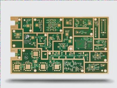
We know that PCBA processing will not always result in a 100% success rate. In such cases, the problematic boards need to be repaired. Today, I will analyze the repair process for everyone.
The Purpose of PCBA Repair and Rework Process
Solder joint defects such as open circuits, bridges, and virtual solders generated in reflow soldering and wave soldering processes require manual trimming with necessary tools (such as BGA rework station, X-ray, and high-power microscope) to eliminate various solder joint defects and ensure the quality of PCBA solder joints. Other tasks involved in the repair process include:
– Repairing missing components
– Replacing components at sticking positions or those that are damaged
– Replacing components after debugging single boards or the entire machine
Solder Joints Requiring Repair
To determine which solder joints need to be repaired, follow these steps:
1. Locate the electronic product and assess which solder joints require attention, based on the product’s classification (Level 3 being the highest standard). Level 3 products demand adherence to the highest testing standards focused on reliability; Level 1 products have more lenient requirements.
2. Understand and adhere to the definition of “good solder joints.” An ideal SMT solder joint should maintain electrical and mechanical strength under expected environmental conditions, usage methods, and lifespan considerations. If a joint meets these criteria, rework may not be needed.
3. Refer to the IPC-A-610E standard for measurement. Solder joints meeting acceptable levels 1 and 2 do not require repair.
4. Inspect per the IPC-A-610E standard. Defects rated 1, 2, and 3 mandate repair.
5. Test according to the IPC-A-610E standard. Warning levels 1 and 2 necessitate repair.


