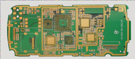
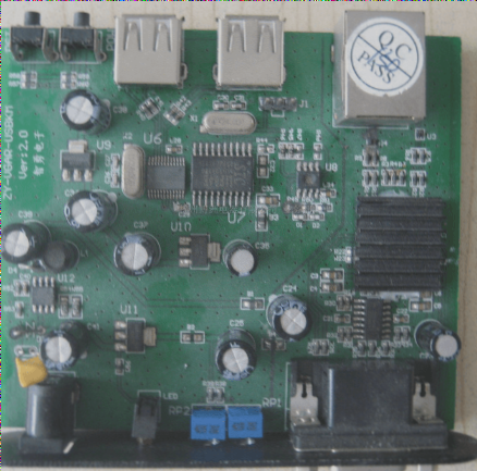
1. There are several methods to create an electroplated layer on the hole wall of a drilled substrate that meets the required standards. This process is referred to as hole wall activation in PCB manufacturing.
2. The commercial production of PCBs involves several intermediate storage tanks, each with its own specific control and maintenance requirements.
3. Through-hole plating is an essential follow-up step after the drilling process. When the drill bit passes through the copper foil and the underlying substrate, the heat generated causes the insulating resin, which makes up the majority of the substrate, to melt. The molten resin, along with other debris from the drilling process, accumulates around the hole and coats the freshly exposed hole wall in the copper foil.
4. This accumulation can negatively affect subsequent electroplating processes. The molten resin also leaves behind a layer of heat-damaged material on the hole wall, which shows poor adhesion to most activators. This issue has led to the development of specialized decontamination and etch-back chemical technologies.

1. A more effective method for prototyping printed circuit boards involves using a specially formulated low-viscosity ink to create a high-adhesion, high-conductivity film on the inner walls of each through hole. This approach eliminates the need for multiple chemical treatments. With just one application step, followed by thermal curing, a continuous film forms on the inner surfaces of all the hole walls, allowing direct electroplating without any further processing. This ink is a resin-based material with strong adhesion properties, enabling it to bond effectively to the walls of most thermally polished holes, thus removing the need for the etch-back step.
2. **Reel-Linkage Selective Plating**
The pins and leads of electronic components, such as connectors, integrated circuits, transistors, and flexible PCBs, utilize selective plating to achieve optimal contact resistance and corrosion resistance. This electroplating process can be performed manually or automatically. Since plating each pin individually is highly costly, batch processing is typically used. Generally, the two ends of a metal foil, rolled to the required thickness, are punched, cleaned using either chemical or mechanical methods, and then selectively plated with materials such as nickel, gold, silver, rhodium, or various alloys like tin-nickel, copper-nickel, or nickel-lead. In selective plating, a resist film is first applied to the areas of the copper foil that do not require electroplating, and electroplating is carried out only on the designated sections.
3. **Brush Plating**
Another form of selective plating is known as “brush plating.” This is an electrodeposition technique where not all parts of the workpiece are immersed in the electrolyte during the process. In brush plating, only specific areas are electroplated, leaving the rest unaffected. This method is often used to plate rare metals onto selected regions of a printed circuit board, such as board edge connectors. Brush plating is particularly useful in the repair of discarded circuit boards in electronic assembly workshops. The process involves wrapping a special anode (typically a chemically inert material like graphite) in an absorbent material, such as a cotton swab, and using it to apply the electroplating solution to the targeted area.


 العربية
 简体中文
简体中文 Nederlands
 English
 Français
 Deutsch
 Italiano
 日本語
日本語 한국어
한국어 Português
 Русский
 Español
 ไทย
ไทย