Share three common types of PCB drilling. PCB drilling is a crucial process in PCB manufacturing, as it involves drilling holes for PCBs, including through holes for wiring, structure, and positioning. Multi-layer PCB drilling is not a one-time task, as some holes are buried in the circuit board while others are drilled through. This requires one drill and two drills to complete the process.
The purpose of PCB drilling is to connect the outer circuit with the inner circuit, and to connect the circuits between different layers. During the later electroplating process, copper plating is applied to the holes to connect the circuits between different layers. Some PCB drilling is also for screw holes, positioning holes, and row holes, each serving different purposes.
The drilling of through holes on the copper clad plate is essential, as these holes provide electrical connections and serve as fixing or positioning devices. There are three common PCB drilling methods: through hole, blind hole, and buried hole, each with unique meanings and characteristics.
Through holes (VIA) are commonly used to conduct or connect copper foil circuits between conductive patterns in different layers of a circuit board. However, they cannot be inserted into copper plated holes of component leads or other reinforcing materials. As PCBs are composed of stacked layers of copper foil with insulation between each layer, the signal connections rely on through holes (via) to communicate between layers.

PCB drilling
The key feature of PCB drilling is the need to plug the conductive holes of the circuit board in order to meet customer requirements. This departure from traditional aluminum sheet plugging processes involves the use of white mesh for resistance welding and plugging holes on the circuit board surface. This results in stable production, reliable quality, and more versatile applications. Conducting holes primarily serve to connect and conduct circuits. With the rapid advancement of the electronics industry, the production process and surface mounting technology for printed circuit boards have seen increased demands. The introduction of the plugging through hole process must meet the following requirements:
1. Copper may be present in the through hole, while solder resistance can either be plugged or left unplugged.
2. The conducting hole must contain a certain thickness requirement of tin and lead (4um), and no solder blocking ink shall enter the hole, which could cause hidden tin beads.
3. Solder blocking ink plug holes are mandatory in conducting holes, which should not be transparent and must not have tin rings, solder beads, or flatness requirements.
Blind holes refer to the connection of the outermost circuit in a PCB with adjacent inner layers through electroplated holes. These holes are called blind holes because the opposite side cannot be seen. The application of blind holes is aimed at increasing the utilization of space between layers in PCB circuits, which are essentially through holes on a surface of the printed circuit board.
Characteristics: Blind holes are located on the top and bottom surfaces of the circuit board with a certain depth, used for connecting the surface circuit and the inner circuit below. The depth of the holes usually does not exceed a certain ratio (aperture). This production method necessitates special attention to the depth of PCB drilling (Z-axis) to be appropriate to avoid difficulties in electroplating inside the holes. Furthermore, it is also possible to drill holes in individual circuit layers that need to be connected beforehand and finally glue them together. However, this requires precise positioning and alignment devices.
Buried holes refer to the connection between any circuit layer inside a PCB that is not conductive to the outer layer, and also refer to conductive holes that do not extend to the surface of the circuit board.
Feature: In this process, PCB drilling after bonding cannot be achieved. PCB drilling must be performed at individual circuit layers, with partial bonding of the inner layer followed by electroplating treatment before complete bonding. This requires more effort than the original through and blind holes, which also makes it the most expensive. This process is usually used for high-density circuit boards to increase the usable space of other circuit layers.
In the PCB production process, PCB drilling is of utmost importance and should not be taken lightly. Improper PCB drilling can result in issues with the through-hole process, affecting the placement and use of devices on the circuit board. In severe cases, the entire PCB could be rendered unusable. Therefore, the PCB drilling process is of crucial importance.
The purpose of PCB drilling is to connect the outer circuit with the inner circuit, and to connect the circuits between different layers. During the later electroplating process, copper plating is applied to the holes to connect the circuits between different layers. Some PCB drilling is also for screw holes, positioning holes, and row holes, each serving different purposes.
The drilling of through holes on the copper clad plate is essential, as these holes provide electrical connections and serve as fixing or positioning devices. There are three common PCB drilling methods: through hole, blind hole, and buried hole, each with unique meanings and characteristics.
Through holes (VIA) are commonly used to conduct or connect copper foil circuits between conductive patterns in different layers of a circuit board. However, they cannot be inserted into copper plated holes of component leads or other reinforcing materials. As PCBs are composed of stacked layers of copper foil with insulation between each layer, the signal connections rely on through holes (via) to communicate between layers.
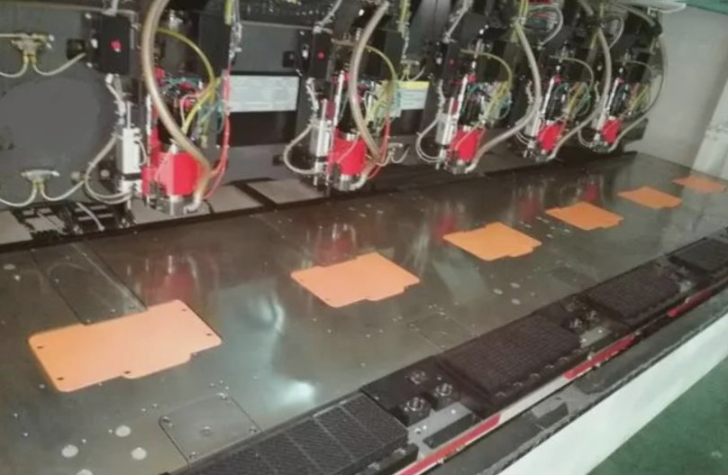
PCB drilling
The key feature of PCB drilling is the need to plug the conductive holes of the circuit board in order to meet customer requirements. This departure from traditional aluminum sheet plugging processes involves the use of white mesh for resistance welding and plugging holes on the circuit board surface. This results in stable production, reliable quality, and more versatile applications. Conducting holes primarily serve to connect and conduct circuits. With the rapid advancement of the electronics industry, the production process and surface mounting technology for printed circuit boards have seen increased demands. The introduction of the plugging through hole process must meet the following requirements:
1. Copper may be present in the through hole, while solder resistance can either be plugged or left unplugged.
2. The conducting hole must contain a certain thickness requirement of tin and lead (4um), and no solder blocking ink shall enter the hole, which could cause hidden tin beads.
3. Solder blocking ink plug holes are mandatory in conducting holes, which should not be transparent and must not have tin rings, solder beads, or flatness requirements.
Blind holes refer to the connection of the outermost circuit in a PCB with adjacent inner layers through electroplated holes. These holes are called blind holes because the opposite side cannot be seen. The application of blind holes is aimed at increasing the utilization of space between layers in PCB circuits, which are essentially through holes on a surface of the printed circuit board.
Characteristics: Blind holes are located on the top and bottom surfaces of the circuit board with a certain depth, used for connecting the surface circuit and the inner circuit below. The depth of the holes usually does not exceed a certain ratio (aperture). This production method necessitates special attention to the depth of PCB drilling (Z-axis) to be appropriate to avoid difficulties in electroplating inside the holes. Furthermore, it is also possible to drill holes in individual circuit layers that need to be connected beforehand and finally glue them together. However, this requires precise positioning and alignment devices.
Buried holes refer to the connection between any circuit layer inside a PCB that is not conductive to the outer layer, and also refer to conductive holes that do not extend to the surface of the circuit board.
Feature: In this process, PCB drilling after bonding cannot be achieved. PCB drilling must be performed at individual circuit layers, with partial bonding of the inner layer followed by electroplating treatment before complete bonding. This requires more effort than the original through and blind holes, which also makes it the most expensive. This process is usually used for high-density circuit boards to increase the usable space of other circuit layers.
In the PCB production process, PCB drilling is of utmost importance and should not be taken lightly. Improper PCB drilling can result in issues with the through-hole process, affecting the placement and use of devices on the circuit board. In severe cases, the entire PCB could be rendered unusable. Therefore, the PCB drilling process is of crucial importance.

