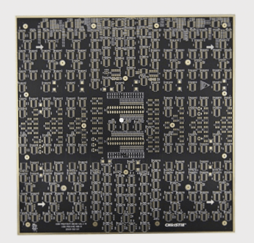
HDI (High-Density Interconnect) boards are among the most precise and complex types of printed circuit boards (PCBs), requiring highly specialized manufacturing processes. The key steps in HDI PCB production include the creation of high-precision circuits, the processing of micro-vias, and the electroplating of surfaces and holes. Below is an overview of these core steps in HDI PCB fabrication.
### 1. Ultra-Fine Circuit Processing
As technology continues to advance, the demand for increasingly miniaturized and sophisticated electronics has placed higher demands on HDI boards. Devices today require ever-finer circuit patterns, with line width and spacing evolving from the early standard of 0.13 mm (5 mil) to 0.075 mm (3 mil), which has now become the industry standard. Leading companies in the HDI PCB sector, such as Shenzhen Benqiang Circuit Co., Ltd., have pushed this further, achieving production capabilities down to 38μm (1.5 mil), approaching the technical limits of the industry.
This evolution of line width and spacing presents a significant challenge to the PCB manufacturing process, particularly in the area of imaging the circuit patterns onto the copper substrate. The question arises: How are these ultra-fine copper traces created?
The process of forming these refined circuits typically involves two key technologies: **laser direct imaging (LDI)** and **pattern etching**.
### Laser Direct Imaging (LDI)
Laser Direct Imaging (LDI) technology plays a crucial role in the creation of precise circuit patterns. In this process, a laser directly scans the surface of the copper-clad laminate that has been coated with a photoresist material. This allows for the direct transfer of the refined circuit pattern without the need for traditional photomasks. LDI technology greatly simplifies the fabrication workflow, providing high accuracy and reducing the potential for defects. As a result, it has become the preferred imaging method in HDI PCB production.
### Conclusion
The fabrication of HDI PCBs is a highly specialized process that demands the latest in technological innovations. As the trend toward smaller, more intricate electronic devices continues, the requirements for HDI boards will only become more stringent. By employing advanced techniques such as laser direct imaging and fine circuit etching, manufacturers can meet these challenges and produce high-performance HDI boards that meet the needs of the most demanding applications.

**1. Semi-Additive and Improved Semi-Additive Methods**
The Semi-Additive Process (SAP) and the Modified Semi-Additive Process (mSAP) are increasingly popular methods for PCB fabrication. These techniques, which fall under the category of pattern etching methods, enable the production of high-resolution conductive traces. Notably, they can achieve line widths as small as 5 micrometers, making them suitable for high-density interconnect (HDI) boards where fine features are crucial. Both SAP and mSAP are considered advanced, precise methods that meet the demanding requirements of modern electronics, particularly in terms of miniaturization and performance.
**2. Micro-Hole Processing for HDI Circuits**
HDI circuit boards are characterized by the use of microvias, which typically have an aperture of 0.10 mm or less. These vias are usually integrated into buried or blind via structures. Currently, the primary method for drilling these tiny holes is laser processing, though CNC (computer numerical control) drilling is also employed in some cases.
Laser drilling offers precision and the ability to create fine microvias, but it has limitations, particularly in terms of hole quality. The laser ablation process can cause discrepancies between the glass fiber and surrounding resin, leading to uneven hole walls. This can compromise the reliability of through-holes, as residual glass fiber filaments may affect the integrity of the connection. In contrast, mechanical (CNC) drilling provides more consistent hole quality, particularly when dealing with materials like epoxy-glass composites.
To address these challenges and improve the reliability and efficiency of PCB drilling, both laser and mechanical drilling technologies are continually being refined. Combining the strengths of each method is key to optimizing the drilling process for HDI boards.
**3. Electroplating and Surface Finishing Techniques**
The quality of electroplating is critical for ensuring the reliability and uniformity of PCB manufacturing. Specifically, enhancing the electroplating process improves both deep hole plating and the overall consistency of metal deposition. This requires continuous refinement of several factors, including the composition of the electroplating solution, the design and maintenance of plating equipment, and the precision of operating procedures.
To achieve better plating results, high-frequency sound waves are now often employed to accelerate the etching process. These sound waves help agitate the plating solution, promoting a more uniform flow of the electroplating material into the holes, particularly in deep vias. Additionally, the inclusion of potassium permanganate in the electroplating bath aids in cleaning the workpiece, improving the overall plating quality. These improvements result in more even copper deposition, which is essential for the reliability of HDI boards.
Another notable advancement is the two-step copper plating method, which is particularly effective for filling blind and through holes with varying diameters and thickness-to-diameter ratios. This technique maximizes copper fill while minimizing the thickness of the surface copper layer, ensuring both electrical performance and physical durability.
In terms of surface finishes, several options are available depending on the application and desired properties. Electroless nickel/gold (ENIG) and electroless nickel/palladium/gold (ENEPIG) are two popular choices for high-end PCBs, offering excellent corrosion resistance, solderability, and overall performance for demanding electronic applications.
By continuously optimizing these processes—ranging from micro-hole drilling to electroplating and surface finishing—PCB manufacturers can enhance the quality and reliability of their boards, meeting the ever-growing demands of modern electronics.
### 1. Ultra-Fine Circuit Processing
As technology continues to advance, the demand for increasingly miniaturized and sophisticated electronics has placed higher demands on HDI boards. Devices today require ever-finer circuit patterns, with line width and spacing evolving from the early standard of 0.13 mm (5 mil) to 0.075 mm (3 mil), which has now become the industry standard. Leading companies in the HDI PCB sector, such as Shenzhen Benqiang Circuit Co., Ltd., have pushed this further, achieving production capabilities down to 38μm (1.5 mil), approaching the technical limits of the industry.
This evolution of line width and spacing presents a significant challenge to the PCB manufacturing process, particularly in the area of imaging the circuit patterns onto the copper substrate. The question arises: How are these ultra-fine copper traces created?
The process of forming these refined circuits typically involves two key technologies: **laser direct imaging (LDI)** and **pattern etching**.
### Laser Direct Imaging (LDI)
Laser Direct Imaging (LDI) technology plays a crucial role in the creation of precise circuit patterns. In this process, a laser directly scans the surface of the copper-clad laminate that has been coated with a photoresist material. This allows for the direct transfer of the refined circuit pattern without the need for traditional photomasks. LDI technology greatly simplifies the fabrication workflow, providing high accuracy and reducing the potential for defects. As a result, it has become the preferred imaging method in HDI PCB production.
### Conclusion
The fabrication of HDI PCBs is a highly specialized process that demands the latest in technological innovations. As the trend toward smaller, more intricate electronic devices continues, the requirements for HDI boards will only become more stringent. By employing advanced techniques such as laser direct imaging and fine circuit etching, manufacturers can meet these challenges and produce high-performance HDI boards that meet the needs of the most demanding applications.
**1. Semi-Additive and Improved Semi-Additive Methods**
The Semi-Additive Process (SAP) and the Modified Semi-Additive Process (mSAP) are increasingly popular methods for PCB fabrication. These techniques, which fall under the category of pattern etching methods, enable the production of high-resolution conductive traces. Notably, they can achieve line widths as small as 5 micrometers, making them suitable for high-density interconnect (HDI) boards where fine features are crucial. Both SAP and mSAP are considered advanced, precise methods that meet the demanding requirements of modern electronics, particularly in terms of miniaturization and performance.
**2. Micro-Hole Processing for HDI Circuits**
HDI circuit boards are characterized by the use of microvias, which typically have an aperture of 0.10 mm or less. These vias are usually integrated into buried or blind via structures. Currently, the primary method for drilling these tiny holes is laser processing, though CNC (computer numerical control) drilling is also employed in some cases.
Laser drilling offers precision and the ability to create fine microvias, but it has limitations, particularly in terms of hole quality. The laser ablation process can cause discrepancies between the glass fiber and surrounding resin, leading to uneven hole walls. This can compromise the reliability of through-holes, as residual glass fiber filaments may affect the integrity of the connection. In contrast, mechanical (CNC) drilling provides more consistent hole quality, particularly when dealing with materials like epoxy-glass composites.
To address these challenges and improve the reliability and efficiency of PCB drilling, both laser and mechanical drilling technologies are continually being refined. Combining the strengths of each method is key to optimizing the drilling process for HDI boards.
**3. Electroplating and Surface Finishing Techniques**
The quality of electroplating is critical for ensuring the reliability and uniformity of PCB manufacturing. Specifically, enhancing the electroplating process improves both deep hole plating and the overall consistency of metal deposition. This requires continuous refinement of several factors, including the composition of the electroplating solution, the design and maintenance of plating equipment, and the precision of operating procedures.
To achieve better plating results, high-frequency sound waves are now often employed to accelerate the etching process. These sound waves help agitate the plating solution, promoting a more uniform flow of the electroplating material into the holes, particularly in deep vias. Additionally, the inclusion of potassium permanganate in the electroplating bath aids in cleaning the workpiece, improving the overall plating quality. These improvements result in more even copper deposition, which is essential for the reliability of HDI boards.
Another notable advancement is the two-step copper plating method, which is particularly effective for filling blind and through holes with varying diameters and thickness-to-diameter ratios. This technique maximizes copper fill while minimizing the thickness of the surface copper layer, ensuring both electrical performance and physical durability.
In terms of surface finishes, several options are available depending on the application and desired properties. Electroless nickel/gold (ENIG) and electroless nickel/palladium/gold (ENEPIG) are two popular choices for high-end PCBs, offering excellent corrosion resistance, solderability, and overall performance for demanding electronic applications.
By continuously optimizing these processes—ranging from micro-hole drilling to electroplating and surface finishing—PCB manufacturers can enhance the quality and reliability of their boards, meeting the ever-growing demands of modern electronics.