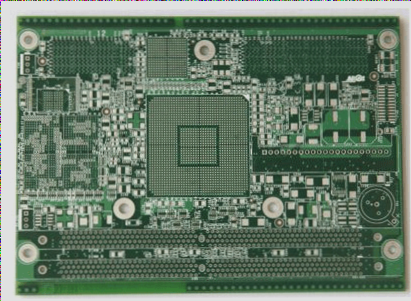
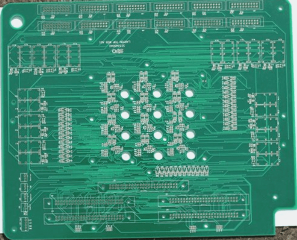
Printed Circuit PCB Board
Printed circuit boards (PCBs) are essential components in electronic devices, facilitating electrical communication through copper-plated pathways called vias. These vias connect the conductive patterns across different layers of the circuit board, allowing for signal transmission within the board.
Modern PCB Manufacturing Innovations
- Innovative methods using white mesh for solder mask and plug hole completion have replaced traditional aluminum plug-hole processes, enhancing production stability and quality.
- Strict requirements in the electronics industry have led to advancements in the via hole plugging process, ensuring optimal performance and reliability.
Types of Holes in PCBs
There are different types of holes in PCBs, each serving a specific purpose:
1. Blind Holes
Blind holes connect the outermost circuit of the PCB to inner layers, maximizing space utilization between circuit layers. These holes are crucial for establishing connections and conducting electrical signals.
- Blind holes are located on the top and bottom surfaces of the circuit board, connecting surface traces with underlying inner traces.
- Precision is key in drilling blind holes, as any deviation can complicate the electroplating process within the hole.
2. Buried Vias
Buried vias connect internal circuit layers but do not extend to the outer layer of the PCB. This labor-intensive process optimizes space utilization in high-density circuit boards.
3. Importance of Drilling
Drilling is a crucial step in PCB production, as it involves creating vias for electrical connections and component mounting. Precision drilling is essential to ensure the reliability and performance of the circuit board.