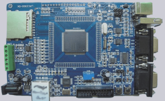
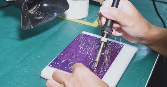
Through-hole technology (also referred to as “thru-hole”) is a mounting method for electronic components, where leads from components are inserted into holes drilled in printed circuit boards (PCBs). These leads are then soldered to pads on the opposite side, either manually or through automated insertion machines.
The quality of the solder joint plays a critical role in the performance of the connection between the component and the PCB. While the appearance of the solder joint is less critical, it typically reflects the overall quality of the joint.
Characteristics
Through-hole mounting provides a strong mechanical bond, especially when compared to Surface-Mount Technology (SMT). However, the additional drilling required to create through-holes increases manufacturing costs. Additionally, the presence of these holes limits the routing space for signal traces, particularly on multi-layer boards where holes must pass through all layers to the opposite side. As a result, through-hole mounting is typically reserved for components such as:
- Bulkier or heavier components like electrolytic capacitors.
- Semiconductors in larger packages (e.g., TO-220) that require additional mounting strength.
- Components like plug connectors or electromechanical relays that need high mechanical support.
Design engineers often prefer through-hole components when prototyping because they are easily inserted into breadboards. However, for high-speed or high-frequency designs, SMT is usually preferred to reduce the effects of stray inductance and capacitance from wire leads, which can interfere with circuit performance. Ultra-compact designs may also necessitate the use of SMT, even in the prototype phase.
Steps in Soldering a Thru-Hole Component
Figures 1-1 through 1-4 illustrate the general steps involved in soldering a thru-hole component. The steps are as follows:
Step 1: Preparation of the Hole and Pad
In this first step, the hole and pad are prepared for soldering. The component lead is placed into or through the hole, ensuring that the lead is positioned above the area where the solder will be applied. This reduces the heat and solder requirements.
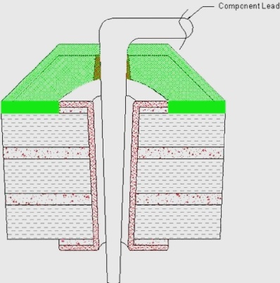
Figure 1-1: Preparing the hole and pad for soldering (Step 1)
Step 2: Applying Heat
Heat is applied evenly to both the lead and the pad/hole, which heats the material and allows the solder to adhere to both surfaces.
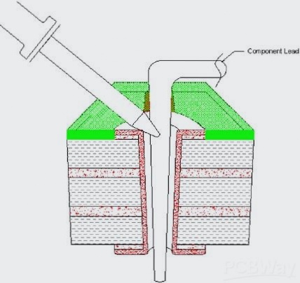
Figure 1-2: Applying heat evenly to the lead and pad/hole (Step 2)
Step 3: Contacting the Iron with Solder
In this step, the solder comes into contact with the tip of the iron, causing it to melt and flow into the hole, creating a proper connection.
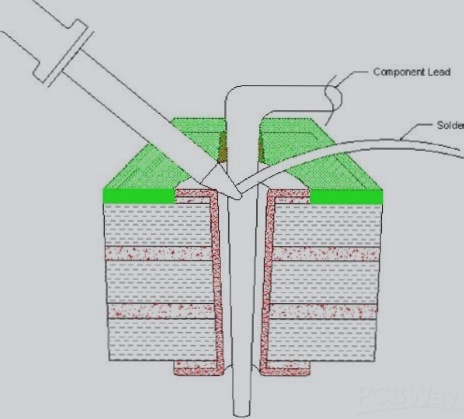
Figure 1-3: Contacting the tip of the iron with the solder (Step 3)
Step 4: Flowing the Solder Through the Hole
The solder flows through the hole, creating a solder mound on both the top and bottom sides. If the soldering is done from the top side, the bottom side should be inspected for sufficient solder and joint quality. In some cases, soldering may be required on both sides to ensure a good connection. Tight clearances inside the hole may necessitate soldering from both sides, which increases the soldering time.
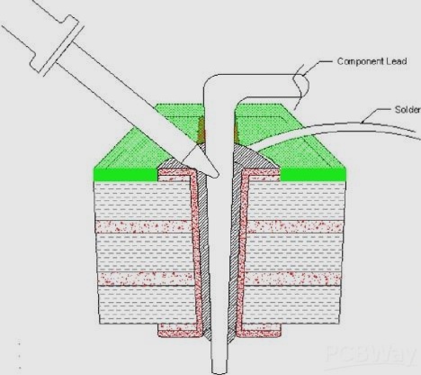
Figure 1-4: Final soldering of the lead (Step 4)
If you have any questions about PCBs or PCBA processes, please feel free to contact us at info@wellcircuits.com.