The Intricacies of Through-Hole and Back Drill Technology in PCB Production
Introduction
PCB designers understand the complexities of through-hole design, but what about the technology behind PCB national control? Let’s explore the technical nuances of PCB through holes and back drills.
Through-Hole Design in High-Speed PCBs
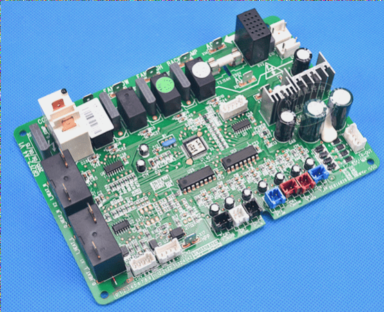
In high-speed PCB design, multi-layer PCBs are commonly used, with through holes playing a crucial role. Through holes in PCBs consist of the hole itself, the soldering plate area surrounding it, and the POWER layer isolation area.
Impact of Through-Holes in High-Speed PCBs
- At frequencies below 1GHz, through holes establish reliable connections with minimal parasitic capacitance and inductance.
- However, at frequencies above 1GHz, the parasitic effects of through-holes become significant, leading to impedance discontinuities and issues like signal reflection, delay, and attenuation.
- Return currents flowing between reference layers through capacitive coupling can cause ground bounce problems.
In high-speed PCB design, through-holes can have negative impacts on circuit design. To mitigate these effects, consider the following measures:
- Opt for appropriate hole sizes based on PCB density.
- Maximize the size of POWER isolation zones.
- Minimize changes to signal routing to reduce the number of holes.
- Use thinner PCBs to reduce parasitic parameters.
- Position power supply and ground pins close to holes with short lead lengths.
- Place grounding through-holes near signal replacement layer through-holes for short-distance loops.
Additionally, through-hole length significantly impacts through-hole inductance. In high-speed PCB design, through-hole length should generally not exceed 2.0mm.
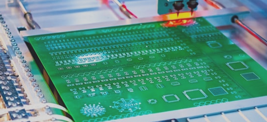
Introduction to Back Drilling Technology in PCB Production
Back drilling in PCB production involves removing excess material from vias to improve signal integrity. This process helps eliminate signal reflections and impedance issues.