(4) The more you focus on the needs of others, the less attention you pay to your own work.
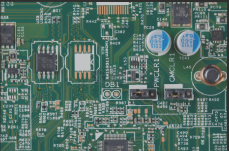
When designing PCBs, it is important to consider the requirements of end users. For instance, when creating a development board, it is beneficial to incorporate more silk screen information on the PCB. This will enhance usability by providing necessary information without the need to constantly refer back to schematics or seek assistance from designers. For mass production products, it is crucial to address issues that may arise during the production process. Ensuring uniformity among devices, appropriate spacing, board edge width, and other factors can streamline the manufacturing process. By addressing these concerns early on, you can minimize disruptions to the design process, reduce the need for future modifications, and decrease the workload for support tasks. While it may seem time-consuming at the outset, taking these considerations into account can ultimately save time in the long run.
If space allows, it is advisable to include more test points on the board to enhance testability. This can expedite the debugging process and provide valuable insights for issue resolution.
(5) Embrace Simulation
Simulation is a valuable tool that some PCB designers may overlook. While it may be tempting to skip simulations and rely on past successes, it is important to recognize that unforeseen issues can arise. Though simulation results may not perfectly align with real-world outcomes, they can reveal trends and guide decision-making. While initially challenging, gradually familiarizing yourself with simulation models and parameters can yield significant benefits. By identifying and addressing potential issues early on, you can preemptively resolve problems before they impact the final design. Investing time in simulations can deepen your understanding of design challenges and enhance your overall proficiency.
(6) Attention to Detail is Key
PCB design demands meticulous attention to detail, requiring carefulness and patience. Novices often encounter errors in device pin assignments, package usage, or pin sequences. While some errors can be rectified with flying leads, others may render a board unusable. Prior to placement on the board, double-check device packages against actual components to avoid common mistakes. Thoroughly reviewing designs is not excessive; it is a proactive measure to prevent avoidable errors. Striving for excellence in design necessitates meticulousness to ensure a clean, efficient PCB layout.
By integrating these principles into your work habits and continually refining your skills, you can achieve greater success in PCB design.
WellCircuits Limited specializes in manufacturing high-precision double-sided, multi-layer, impedance-controlled, blind/buried vias, and heavy copper circuit boards. Our product range includes HDI, heavy copper, backplanes, rigid-flex assemblies, embedded capacitors and resistors, gold fingers, and other specialized circuit boards to meet diverse customer needs.

