PCB Design Best Practices
- Use Advanced Design Software
- Optimize Component Placement and Routing
- Follow Design Guidelines and Standards
- Simulate and Test Designs
- Design Rules and Limitations
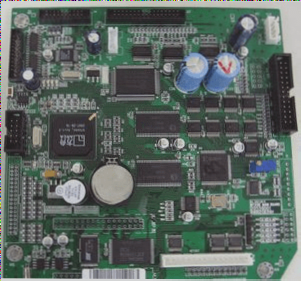
- Component Layout
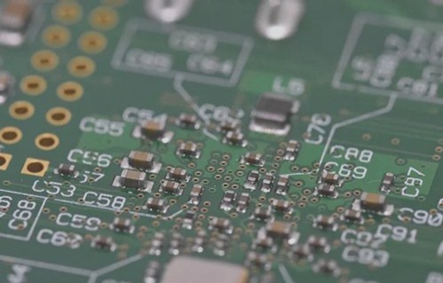
- Fan Out Design
- Manual Wiring and Key Signal Processing
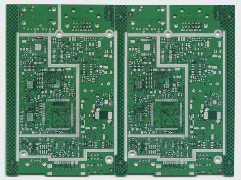
- Automatic Routing
Choosing the right PCB design software with features like automatic routing and signal integrity analysis is essential for efficient and accurate designs.
Strategically placing components and routing traces can minimize errors and improve signal integrity, thermal management, and impedance matching.
Adhering to industry standards like IPC-2221 and IPC-2222 ensures reliability and prevents manufacturing issues in PCB fabrication.
Using simulation tools to analyze signal integrity and testing prototypes in real-world conditions helps identify and resolve design issues early.
Setting rules for wire width, vias, parallelism, and layer restrictions is crucial for successful routing and optimal performance.
Optimizing component layout based on design for manufacturability rules can enhance automatic wiring and prevent interference.
Ensuring each pin of surface mount devices has vias facilitates internal connections and testing, especially for additional connections.
Manually routing key signals before automatic wiring helps optimize paths and prevent common impedance interference.
Using automatic routing tools while controlling electrical parameters like distributed inductance can streamline the design process.
Optimizing Wiring Arrangement for PCB Design
When dealing with signals that have minimal constraints and lengthy wiring, it is crucial to identify the optimal wiring paths to minimize signal length and decrease the number of vias on the PCB board. This manual editing process can significantly enhance the overall performance and efficiency of the circuit.