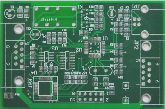
In PCB design, engineers inevitably encounter various challenges. The following summarizes ten common issues in PCB design, aiming to help everyone avoid these pitfalls:
1. Misplaced Components:
1. Components covering SMD pads hinder PCB testing and component soldering.
2. Characters designed too small cause screen printing issues; too large, they overlap and are indistinct.
2. Overuse of Graphic Layers:
1. Unnecessary lines on graphic layers can confuse; more layers designed than necessary.
2. Simplify design but ensure clarity; use Protel software to draw and mark lines correctly.
3. Non-standard designs like top-layer components or bottom-layer soldering cause inconvenience.
3. Pad Overlaps:
1. Pad overlap (beyond the pad surface) can damage drills during manufacturing.
2. Overlapping holes in multi-layer boards can lead to production scrap.
4. Single-Sided Pad Aperture Settings:
1. Single-sided pads without drills should be marked with zero aperture.
2. Clearly mark special drilling needs for single-sided pads.
5. Confusion between Power and Signal Pads:
Designing power pads inverted to the actual PCB image causes isolation line confusion, risking short circuits. Ensure isolation lines for power groups are clear to prevent accidental connection or isolation.
6. Using Fill Blocks for Pads:
Using filler blocks for pads passes DRC but complicates processing. Solder may cover fill blocks during soldering, affecting device performance.
7. Unclear Processing Layer Definitions:
1. Single-sided design without layer polarity instructions can lead to faulty installation and soldering.
2. Sequential layer designs (e.g., TOP, MID1, MID2, BOTTOM) must follow processing sequence to avoid errors.
These corrections streamline the text for clarity and technical accuracy in PCB design discussions.

8. Too many filling blocks in the design or filling blocks with extremely thin lines can lead to data loss or incomplete light drawing data.
9. Surface mount device (SMD) pads that are too short pose challenges during testing. In densely packed SMDs, where the pin spacing is minimal and pad sizes are small, test needle installation requires careful staggering (vertically and horizontally). Short pads, while not affecting device installation, can lead to incorrect test needle placement.
10. The spacing between grid lines in large area grids should not be too small (less than 0.3mm). During PCB manufacturing, narrow gaps between grid lines can cause film debris to adhere to the board after the etching process, potentially resulting in wire breakage.
1. Misplaced Components:
1. Components covering SMD pads hinder PCB testing and component soldering.
2. Characters designed too small cause screen printing issues; too large, they overlap and are indistinct.
2. Overuse of Graphic Layers:
1. Unnecessary lines on graphic layers can confuse; more layers designed than necessary.
2. Simplify design but ensure clarity; use Protel software to draw and mark lines correctly.
3. Non-standard designs like top-layer components or bottom-layer soldering cause inconvenience.
3. Pad Overlaps:
1. Pad overlap (beyond the pad surface) can damage drills during manufacturing.
2. Overlapping holes in multi-layer boards can lead to production scrap.
4. Single-Sided Pad Aperture Settings:
1. Single-sided pads without drills should be marked with zero aperture.
2. Clearly mark special drilling needs for single-sided pads.
5. Confusion between Power and Signal Pads:
Designing power pads inverted to the actual PCB image causes isolation line confusion, risking short circuits. Ensure isolation lines for power groups are clear to prevent accidental connection or isolation.
6. Using Fill Blocks for Pads:
Using filler blocks for pads passes DRC but complicates processing. Solder may cover fill blocks during soldering, affecting device performance.
7. Unclear Processing Layer Definitions:
1. Single-sided design without layer polarity instructions can lead to faulty installation and soldering.
2. Sequential layer designs (e.g., TOP, MID1, MID2, BOTTOM) must follow processing sequence to avoid errors.
These corrections streamline the text for clarity and technical accuracy in PCB design discussions.
8. Too many filling blocks in the design or filling blocks with extremely thin lines can lead to data loss or incomplete light drawing data.
9. Surface mount device (SMD) pads that are too short pose challenges during testing. In densely packed SMDs, where the pin spacing is minimal and pad sizes are small, test needle installation requires careful staggering (vertically and horizontally). Short pads, while not affecting device installation, can lead to incorrect test needle placement.
10. The spacing between grid lines in large area grids should not be too small (less than 0.3mm). During PCB manufacturing, narrow gaps between grid lines can cause film debris to adhere to the board after the etching process, potentially resulting in wire breakage.