Exploring the Benefits of 8-Layer PCBs
From household appliances to medical devices, printed circuit boards (PCBs) play a crucial role in various technologies. Among them, the 8-layer PCB has gained popularity for its unique advantages and applications.
Understanding 8-Layer PCBs
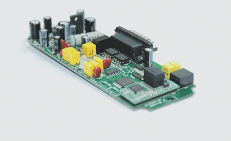
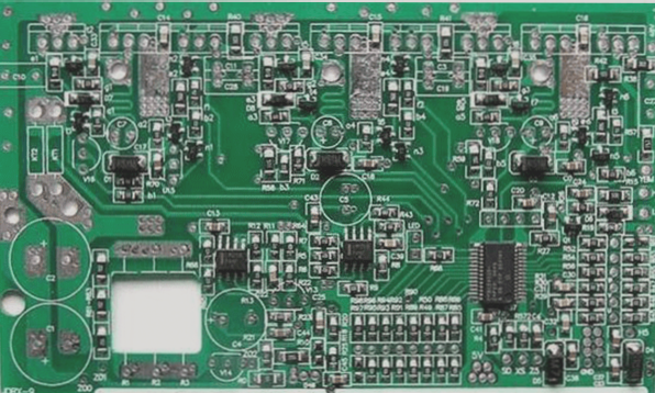
An 8-layer PCB consists of eight tightly integrated layers, offering extensive routing capabilities and electromagnetic compatibility. These PCBs are commonly found in devices like digital cameras, cell phones, and motherboards due to their compact size and robust design.
Design and Fabrication
Designing a high-quality 8-layer PCB requires meticulous material selection and adherence to best practices. The intricate stack-up design ensures comprehensive fulfillment of all requirements, enhancing performance and functionality.
Advantages of 8-Layer PCB Stack-Up
- Enhanced Security: 8-layer PCBs reduce vulnerability to external influences, enhancing overall device performance.
- Radiation Minimization: These PCBs minimize electromagnetic interference radiation, ensuring sustained high performance.
- Cost Efficiency: Despite being slightly more expensive, 8-layer PCBs offer extended usability and superior performance.
- Performance Enhancement: Opting for an 8-layer PCB guarantees improved device longevity and performance.
Applications of 8-Layer PCBs
8-layer PCBs find extensive use in various industries, including medical, automotive, manufacturing, and more, due to their reliability, high performance, and longevity.
Factors Affecting Cost
- Board Size: Larger boards with numerous components incur higher costs due to increased assembly complexity.
- Thickness: Thicker boards with more components generally cost more to manufacture.
- Surface Finish: High-quality surface finishes enhance durability and performance, impacting production costs.
For those considering the benefits of 8-layer PCBs, understanding their design, advantages, and applications is essential for making informed decisions in various industries.
Essential Guidelines for Designing an 8-Layer PCB
- Precise Routing Paths: Clear routing paths reduce interference issues.
- Ground Plane Configuration: Proper ground plane placement prevents malfunctions.
- Efficient Return Paths: Well-defined return paths eliminate interference.
- Vias Utilization: Use buried or blind vias for optimized routing.
The Design Process for an 8-Layer PCB
- Planning Phase: Select type, components, dimensions, and layout details.
- Component Integration: Implement constraints during integration.
- Component Placement: Position components for optimal performance.
Common Applications of 8-Layer PCBs
8-layer PCBs are used in medical, aviation, automotive, and more to create compact devices like digital cameras and cell phones.
Surface Finish Recommendations
For best performance, consider finishes like Hot Air Solder Leveling or Electroless Nickel Immersion Gold.
Cost Factors for 8-Layer PCBs
Board size, thickness, surface finish, hole specs, and customization impact costs.
Benefits of 8-Layer PCBs
8-layer PCBs offer extended shelf life, exceptional performance, and unmatched reliability.
For top-quality 8-layer PCBs, consult experienced manufacturers for optimal results.