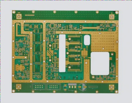
Understanding Transmission Lines in High-Speed PCB Design
Before delving into high-speed PCB design, it’s crucial to grasp the concept of transmission lines. In PCBs, signal reflection can occur due to traces with specific impedance. When the line’s impedance doesn’t match the output terminal, signal reflection arises, leading to potential malfunctions. Understanding transmission lines is key to addressing these issues.
Exploring Transmission Lines
A transmission line comprises a signal path and a corresponding signal return path, typically consisting of two conductors on a PCB. The trace on the PCB is the most common form of a transmission line. When analyzing transmission lines, considering the return path is essential, as a single conductor alone cannot serve as a transmission line.
- Transmission lines are idealized circuit elements, distinct from resistance, capacitance, and inductance. They exhibit unique characteristics, making them suitable for simulation purposes.
- Characteristic impedance and time delay are two vital attributes of transmission lines, influencing signal integrity within circuits.
Key Concepts in High-Speed PCB Design
Transmission Line Impedance
Impedance, characteristic impedance, and instantaneous impedance are terms often encountered in transmission line discussions. While technically different, they are frequently treated similarly. Characteristic impedance, describing the impedance experienced by signals along the line, is critical for maintaining signal integrity.
Transmission Delay
Time delay, or time delay (TD), signifies the duration for a signal to traverse the transmission medium. Propagation delay (PD) is the time for a signal to pass through a unit length of the medium, inversely proportional to the propagation speed.
Time delay = Propagation delay × Transmission length (L)
Structural Components of PCB Transmission Lines

In a PCB, transmission line structures consist of traces within or near dielectric materials, often with reference planes. Copper and FR4 glass fiber are common materials used. Microstrip and stripline are prevalent transmission line types in digital design.
Microstrip lines, found on the outer layer, have one reference plane, while stripline traces are sandwiched between two planes on inner layers. Understanding these structures is vital for effective high-speed PCB design.
Mastering High-Speed PCB Design
By comprehending transmission lines’ behavior, particularly in high-speed PCB design, one can mitigate issues like signal reflection and timing delays. This knowledge is essential for ensuring optimal system performance and functionality.
What Defines a Transmission Line?
Understanding Transmission Lines in PCB Design
- A transmission line on a PCB consists of two conductors, one for signal propagation and the other for signal return.
- When analyzing a transmission line, considering the return path is essential as a single conductor does not form a transmission line.
- Characteristics of a transmission line include impedance and time delay.
Key Concepts of Transmission Lines
Impedance, characteristic impedance, and instantaneous impedance are terms often used interchangeably:
- Impedance at the start of a transmission line is known as impedance.
- Instantaneous impedance is the impedance encountered by the signal at any moment.
- Characteristic impedance is the constant instantaneous impedance along the transmission line, crucial for signal integrity.
Understanding Transmission Delay
Transmission delay refers to the time taken for signals to travel the entire length of the transmission medium on a PCB. It includes propagation delay, which is the delay over a unit length of the medium.
Time Delay = Propagation Delay × Transmission Length (L)
Structure of PCB Transmission Lines
In PCB design, transmission lines are typically composed of traces in or near insulating materials, with copper as the primary metal and FR4 as the dielectric material. The two main types of transmission lines are microstrip and stripline.
Microstrip lines are on the outer layer with one reference plane, while stripline is sandwiched between two reference planes on inner layers.
If you have any PCB-related questions, feel free to reach out to us at info@wellcircuits.com.


