PCB Circuit Board Design Guidelines
PCB circuit boards, also known as Printed Circuit Boards (PCBs), are essential for connecting electronic components and integrating functions in power supply circuit design.
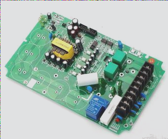
Basic Rules for Component Layout:
- Layout components based on circuit modules to group related circuits with similar functions.
- Avoid placing components near non-mounting holes and maintain proper distances around mounting holes to prevent interference.
- Avoid placing via holes directly beneath certain components to prevent short-circuiting.
- Maintain proper distances between components and board edges.
- Ensure proper spacing between component pads.
- Keep metal shell components away from other components and printed traces.
- Position heating elements away from heat-sensitive components.
- Position power sockets strategically for easy cable management.
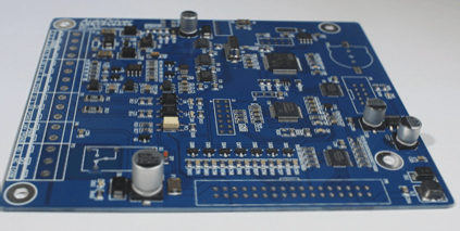
Arrangement of Other Components:
- All IC components should be aligned on one side.
- Ensure clear polarity markings for polar components.
- Opt for dense and uniform board surface wiring.
- Avoid through-holes on PCB patch pads.
- Align patch components consistently.
- Consistent orientation for polarized devices.
Component Wiring Rules:
- Avoid wiring near the PCB edge and around mounting holes.
- Ensure proper widths for power and signal lines.
- Follow specific guidelines for different components.
- Optimize power and ground line layouts for better performance.
Improving Anti-Interference Ability:
Developing electronic products with processors requires attention to anti-electromagnetic interference, especially in systems with high clock frequencies, high-power circuits, and weak analog signal circuits.