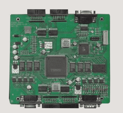
The Latest in PCB Fabrication: SMOBC Process and Plugging Method
The SMOBC process for pattern electroplating, lead, and tin stripping in PCB fabrication involves a series of steps that ensure a high-quality final product. After etching, the process includes lead and tin removal, inspection, cleaning, solder mask patterning, nickel plating, gold plating plugging, and more.
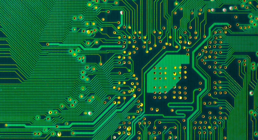
Main Process Flow for Plugging Method:
- Double-sided foil-clad board
- Drilling
- Chemical copper plating
- Copper plating on entire PCB board
- Hole blocking
- Screen print imaging (positive image)
- Etching
- Remove screen print material and block material
- Cleaning
- Solder mask patterning
- Nickel plating, gold-plating plugging
- Tape plugging
- Hot air leveling
The plugging method focuses on efficiently plugging holes and washing the ink used for plugging. An alternative method, the masking hole process, involves using special masking dry film to cover holes instead of hole plugging ink and screen print imaging. While this eliminates the need to clean ink in the holes, it requires a higher level of precision in applying the masking dry film.