Understanding Microvias in Printed Circuit Boards
Introduction to Microvias
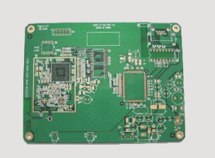
With the rise of smart technology, printed circuit boards (PCBs) are becoming more prevalent in devices and gadgets. Advanced PCBs with multiple layers are ideal for sophisticated gadgets with numerous features. Microvias are tiny holes that connect the layers of a multi-layer PCB, ensuring uninterrupted interconnection.
Exploring Types of Microvias
- Microvias typically have a standard aspect ratio of 2:1, limiting their ability to connect only two board layers. Unlike plated-through holes (PTHs) with a higher aspect ratio of 10:1.
- The neck region of a microvia is prone to damage from constant mechanical shock or vibration.
Understanding these characteristics is crucial before incorporating microvias into a circuit. Below are the common types of microvias found in PCBs:

Blind Microvias
Blind microvias start from the surface layer of the circuit and extend one to two layers below. They are most effective when connecting the surface to a single layer underneath, not suitable for connecting multiple layers.
Buried Microvias
Buried microvias do not touch the circuit’s surface at any point. Similar to blind microvias, they offer durability and optimal performance when connecting single layers.
Stacked Microvias
Stay tuned for more insights on stacked microvias in PCBs.
Advantages of Stacked Microvias
- Stacked microvias, composed of multiple buried microvias, are ideal for interconnecting multiple layers in a PCB.
- Microvias are space-efficient, saving room on the board and reducing the need for larger circuits.
- Utilizing microvias lowers the risk of manufacturing defects and eases the fabrication process.
- In high-speed circuits like HDI, microvias minimize radiation compared to larger vias, enhancing signal integrity.
- Microvias have shorter trace lengths, making them more reliable and improving RF capability.
Capabilities of Microvias in PCBs
- Microvias facilitate connections between different layers of a printed circuit board.
These advantages highlight why microvias are superior to larger holes, enhancing PCB quality and functionality across various board sizes and speeds.
The Benefits of Microvias in PCB Design
- When it comes to PCB design, via-in-pad microvias offer a unique advantage by being placed directly on the solder pads. This feature plays a crucial role in shrinking the size of the circuit board, ensuring its functionality and condition are maintained.
- Engineers and technicians can utilize microvias to design circuit boards with smaller BGA pitches, as opposed to traditional methods that require larger pitches for bigger holes. Microvias, with their small sizes, eliminate the need for bigger BGA pitches, allowing for more compact designs.
- Microvias enable high wiring density, making them a cost-effective solution for increasing the density of a PCB. By using microvias, you can achieve a higher level of wiring density efficiently.
- Reliability is a key factor in PCB performance, and microvias excel in maintaining thermo-mechanical reliability. The use of microvias ensures the stability and functionality of circuit boards, contributing to their overall reliability.
- Microvias pave the way for future-oriented technology by allowing for smaller and more compact circuit board designs. As technology advances towards miniaturization, microvias play a significant role in reducing the size of devices and gadgets, shaping the future of technology.
- Addressing inductance and capacitance effects in circuits can be challenging, but microvias simplify the process by reducing these effects. By controlling these effects effectively, microvias enhance the performance of other circuit components, showcasing their beneficial impact on PCBs.
Key Takeaway:
Explore the advantages of microvias in PCB design and how they can optimize circuit performance. For further inquiries or tailored solutions regarding microvias, feel free to contact our expert team for assistance.