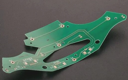
Types of PCB Vias and Their Advantages
-
Blind Vias
Blind vias are located on the top and bottom surfaces of the circuit board, connecting surface traces to inner layer traces. The depth and diameter of blind holes adhere to specific ratios for manufacturability.
-
Buried Vias
Buried vias are entirely within the inner layers of the PCB and do not extend to the outer surfaces. They are prepared during the layer buildup process and are common in multilayer PCBs.
-
Through Vias
Through-holes extend completely from one layer to another, enabling internal connections and serving as mounting holes for components. They are cost-effective and simpler to implement in printed circuit boards.
Advantages of Blind and Buried Vias

-
Size and Cost Efficiency
Blind and buried vias reduce the size and number of circuit board layers, improving electromagnetic compatibility, reducing customization costs, and enhancing product characteristics.
-
Dense Packing Considerations
Using numerous through-holes can hinder inner wiring in multi-layer circuit boards, disrupting impedance characteristics and functionality, especially when passing through power and ground layers.
-
Customized Design
Designing vias should align with specific product requirements; not all multilayer circuit boards require blind or buried vias.