The choice of PCB surface treatment process largely depends on the type of final assembly components, as it impacts the production, assembly, and final use of the PCB. Below, we will specifically introduce five common surface treatment processes.

1. Hot Air Leveling

Hot air leveling was once the dominant method in PCB surface treatment. In the 1980s, it was used for more than three-quarters of PCBs. However, over the past decade, the industry has been shifting away from this process. Currently, it is estimated that only about 25% to 40% of PCBs utilize hot air leveling. Although the process is effective, it is also messy, unpleasant, and hazardous, which makes it less favored. Despite these drawbacks, hot air leveling is particularly suited for larger components and wires with wider spacing. In high-density PCBs, the flatness achieved by hot air leveling can impact subsequent assembly, which is why HDI boards generally avoid using this method.

1. With the advancement of technology, the industry now has a hot air leveling process suitable for assembling QFPs and BGAs with smaller pitches, but its practical applications are limited. Currently, some factories use organic coating and electroless nickel/immersion gold processes instead of hot air leveling; technological developments have also led some factories to adopt tin and silver immersion processes. Coupled with the lead-free trend in recent years, the use of hot air leveling has been further restricted. Although lead-free hot air leveling has emerged, it may involve equipment compatibility issues.

2. Organic coating

It is estimated that about 25%-30% of PCBs currently use organic coating technology, and this proportion has been rising (organic coating may have now surpassed hot air leveling). The organic coating process is suitable for both low-tech and high-tech PCBs, such as those for single-sided TVs and high-density chip packaging. For BGAs, organic coating is also increasingly used. If the PCB does not have specific functional requirements for surface connection or constraints on storage period, organic coating is an ideal surface treatment process.

3. Electroless nickel plating/immersion gold

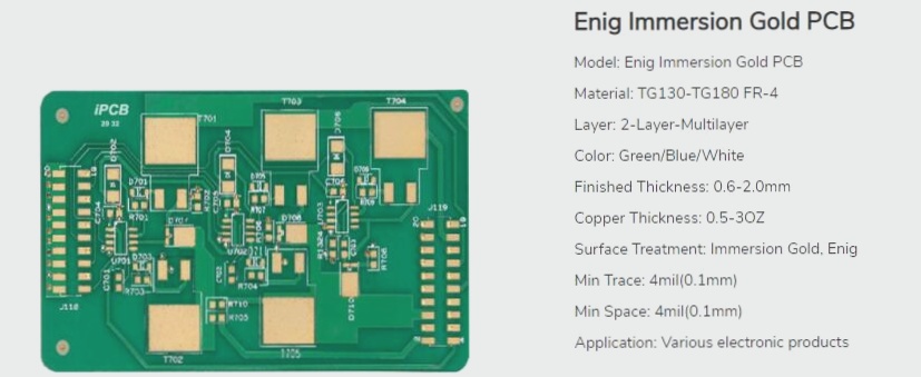
The electroless nickel/immersion gold process differs from organic coating and is mainly used for boards with functional connection requirements and long storage periods, such as mobile phone keypads, edge connections in router housings, and chip processor connections. Due to hot air leveling’s flatness issues and the removal of organic coating flux, electroless nickel/immersion gold was widely used in the 1990s. However, the emergence of black plates and brittle nickel-phosphorus alloys led to a decline in its use. Yet, almost every high-tech PCB factory now employs this process. Considering the brittleness of solder joints formed with copper-tin intermetallic compounds, portable electronics (like mobile phones) predominantly use organic coating, immersion silver, or immersion tin for solder joints, with electroless nickel/immersion gold reserved for key areas, contact points, and EMI shielding. It is estimated that about 10%-20% of PCBs currently use electroless nickel/immersion gold processes.

4. Immersion silver

Immersion silver is more cost-effective than electroless nickel/immersion gold. For PCBs with functional connection requirements and a need to cut costs, immersion silver is a good choice due to its excellent flatness and contact properties. Immersion silver is widely used in communication products, automobiles, computer peripherals, and high-speed signal designs. It offers superior electrical properties for high-frequency signals. EMS recommends immersion silver for its ease of assembly and better checkability. However, due to issues like tarnishing and solder joint voids, immersion silver’s growth has been slow but not decreasing. It is estimated that about 10%-15% of PCBs currently use immersion silver.

5. Immersion tin

Introduced in the past decade, immersion tin arose from the need for production automation. Immersion tin does not introduce any foreign elements into the soldering area, making it suitable for communication backplanes. However, tin’s solderability diminishes beyond the board’s storage period, necessitating better storage conditions. The use of immersion tin has also been restricted due to carcinogenic substances involved. It is estimated that about 5%-10% of PCBs currently use immersion tin.

The future direction of PCB surface treatment processes remains uncertain. With increasing customer demands, stricter environmental regulations, and a growing array of surface treatment options, choosing processes with development potential and versatility can be overwhelming. Nonetheless, meeting customer requirements and environmental protection must remain the top priorities.
Please enable JavaScript in your browser to complete this form.

Quick Quote

Info
Click or drag a file to this area to upload.
send me gerber or pcb file,format:7z,rar,zip,pdf