PCB Design: Common Issues and Best Practices
Introduction
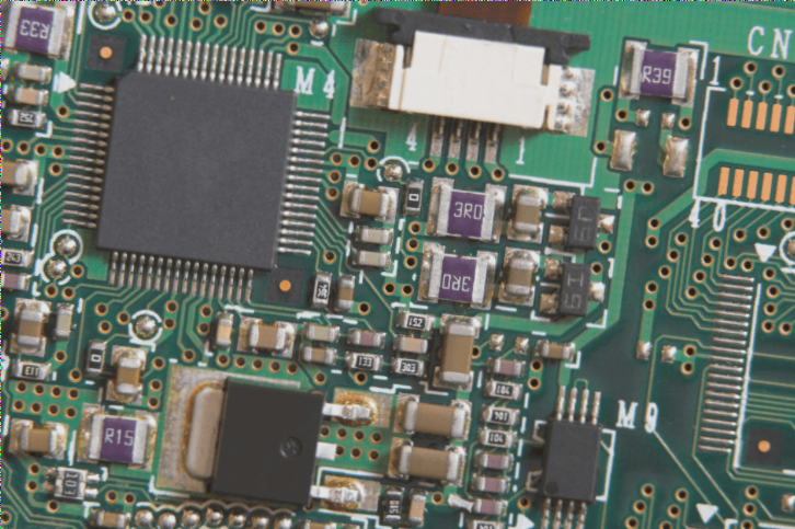
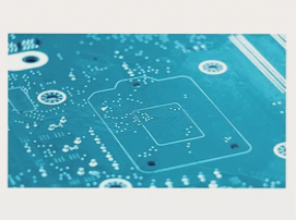
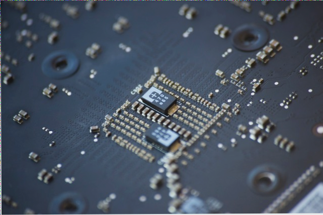
PCB design is a complex task that involves translating circuit schematics into functional printed circuit boards. It requires a deep understanding of circuit theory and manufacturing processes to meet design requirements successfully.
Key Issues in PCB Design
1. Pad Overlap
Issue: Pad overlap, especially in non-surface-mount pads, can lead to drilling hole conflicts during fabrication, risking damage to vias or pads.
Solution: Verify pad layouts, especially in multi-layer designs, and use design rule checks to prevent overlap.
2. Misuse of Graphics Layers
Issue: Adding unnecessary connections to graphics layers can cause confusion and potential short circuits if not managed correctly.
Solution: Use graphics layers only for non-electrical elements, manage layer visibility, and double-check layer selection before fabrication.
Best Practices for PCB Designers
Addressing common issues like pad overlap and graphics layer misuse is crucial to reduce errors in manufacturing. Designers should run design rule checks and maintain clear layer management for successful PCB production.
Additional Insights
In PCB design, errors like violating conventional practices and random placement of text and symbols can impact manufacturing and functionality. Adhering to systematic guidelines for component placement and text sizing is essential for a smooth production process.
Conclusion
By following best practices and avoiding common pitfalls in PCB design, designers can minimize costly mistakes and ensure a seamless transition from design to production.
Common PCB Design Issues and Best Practices
1. Violations of Conventional Design Practices: Incorrect component placement can complicate manufacturing and disrupt board functionality.
2. Random Placement of Text and Symbols: Following guidelines for text and symbol placement is crucial to avoid manufacturing and inspection issues.
3. Single-Sided Pad Aperture Design
Single-Sided PCB Design Best Practices
- Single-sided pads usually do not need drilling, but if drilling is necessary, mark the aperture as “zero diameter” to avoid confusion.
- Explicitly mark drilled single-sided pads to ensure correct processing during production.
Common Mistakes to Avoid in PCB Design
-
Filler Blocks in Pad Design
Using filler blocks for DRC can lead to solder mask generation issues, hindering proper component soldering.
-
Ground and Power Planes Design
Designing power planes as “flower pads” can cause connectivity problems, impacting signal transmission and power delivery.
-
Unclear Processing Levels
Define processing levels clearly, especially in multi-layer boards, to avoid confusion during fabrication.
-
Overuse of Filler Blocks or Thin Lines
Excessive filler blocks or thin lines can result in lost Gerber data and processing complications.
-
Inadequate SMD Pad Size
Ensure SMD pad sizes are sufficient for testing and soldering in dense layouts to prevent manufacturing issues.
-
Insufficient Grid Spacing in Large Areas
Maintain proper spacing in large copper fills to avoid film breakage during the manufacturing process.
-
Distance Between Copper Areas and Outer Frame
Maintain a minimum gap between large copper areas and the PCB’s outer frame to prevent warping and solder mask problems.
-
Outline Design Consistency
Ensure clear and consistent contour lines to avoid errors in the final product during PCB fabrication.
-
Even Pattern Design
Uniform pattern design is crucial to prevent plating issues that can affect the PCB’s performance.
-
Copper Area Size and Grid Use
Use grid lines for large copper areas to prevent thermal issues during SMT assembly.
Optimizing PCB Design for Manufacturing Success
When it comes to PCB design, avoiding common pitfalls and following best practices is key to a successful manufacturing process. Every decision made, whether it’s determining pad sizes or managing copper areas, significantly impacts the functionality and reliability of the end product.
Attention to detail, rigorous testing, and effective communication with the manufacturing team are crucial components in ensuring a high-quality PCB design. By incorporating these strategies, designers can minimize errors, streamline production, and ultimately enhance the overall quality of their designs.