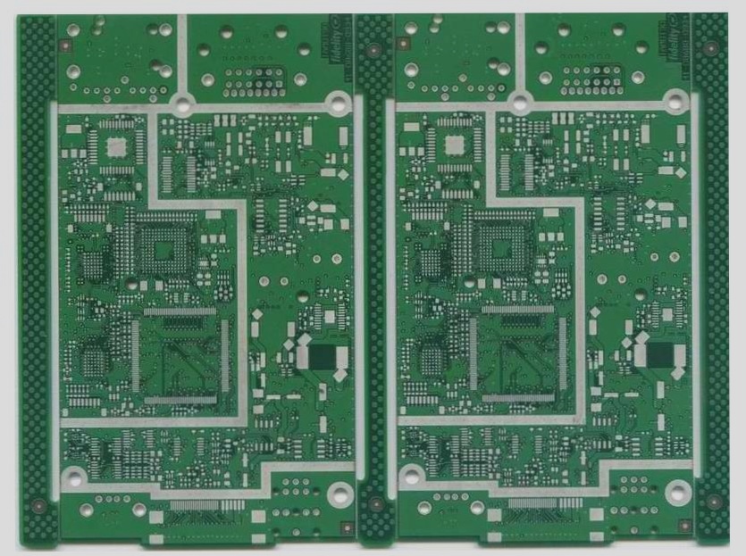
Today, ultra-low-cost hybrid tuner for single-layer PCB board design and most tuners in TV and video converter box applications use the traditional single-conversion MOPLL concept. Such tuners can process both analog and digital TV signals, or both (so-called hybrid tuners). Key factors to consider when designing such a tuner include low cost, low power consumption, small size, and choice of external components. This single-chip ULC tuner integrates RF and IF circuits and can operate at 5V or 3.3V with 34% lower power consumption. The design uses a single-layer PCB board, which further reduces the system cost, and can handle mixed signals such as DVB-T/PAL/SECAM, ISDB-T/NTSC and ATSC/NTSC, and can support almost all regional standards. The tuner is actually not only an RF tuner, but also a half NIM because it includes an IF module. The RF input signal is separated by a simple high-pass filter plus a combination of IF and civil band (CB) notch filters. Instead of using PIN diodes for frequency band switching, this design uses a very simple triplex circuit for frequency band switching. The antenna impedance is transformed to the tuned input circuit through a high inductance coupling circuit. The BG5120K dual MOSFET can be used for both VHF bands. In the following tuned bandpass filter circuit, channel selection and suppression of unwanted signals such as adjacent channels and video frequencies are performed. The pre-stage tracking notch filter and the capacitive image frequency compensation circuit of the band-pass filter are specially used to suppress the image frequency.
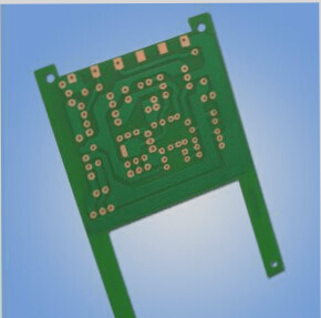
The TUA6039-2 is a complete tri-band tuner IC that includes all required active components such as 3 mixers, 3 oscillators, 1 SAW driver, and 1 IF amplifier. The complete PLL function includes 4 PNP ports and one NPN port for band switching and a wideband AGC detector as an internal tuner AGC. Combined with loop filters, 4 programmable charge pump current circuits, balanced crystal oscillators, and voltage controlled oscillators, this half NIM achieves phase noise performance suitable for all digital devices. The balanced IF output signal of the TUA6039-2 can directly drive the SAW filter in the subsequent IF circuit. Then, the signal output by the SAW is further amplified by a gain-controlled on-chip amplifier, and the amplified output signal can be directly used in the subsequent demodulator. The conversion of RF to IF is also done inside the chip. The power consumption of this half NIM is less than 130mA at +5V supply voltage, and the power consumption is less than 650mW. If the +3.3V power supply is used, the total power is only 429mW. This significant savings in power consumption is a great advantage for portable or handheld devices. The design of ULC tuners with a single-layer PCB has been widely accepted by customers. In the competitive TV tuner market, any cost improvement could further reduce production costs. Therefore, any cost difference between a single-layer PCB board and a double-layer PCB board is very important to the overall BOM (bill of materials) of the tuner. This half NIM design uses a single-sided FR4 PCB with a thickness of 1.6mm.
In the mixed reception of standard TV signals such as PAL/DVB-T, NTSC/ATSC, NTSC/ISDB-T, etc., this reference design developed on a single-layer PCB board shows good performance, it can handle T-DMB, DAB, DMB-TH, DVB-C and Open Cable and other standards. In this design, it is necessary to use the PLL loop filter and the post filter configuration. The 62.5kHz reference frequency rejection ratio depends on the configuration of the different loop filters and their post filters. Although the loop filter can be modified to cover the two reference frequencies of 166.67kHz and 62.5kHz in mixed mode, there is always a tradeoff between the performance of phase noise, reference frequency rejection, and PLL lock time. Therefore, it is strongly recommended that the designer select the reference frequency (62.5kHz or 166.67kHz or both) before applying the corresponding loop filter and post filter configuration. The measurement results show that the single-layer PCB board tuner design can achieve 60dB or even higher reference frequency rejection performance in mixed reception mode, which is sufficient to meet the strict requirements of analog receivers.
One of the challenges in developing the reference design is how to place the chip’s VQFN package on the PCB. Connecting and grounding on a single-layer PCB reduces grounding flexibility. Grounding is very important in RF design, which is a challenge for tuner designers. Several key electrical parameters affected by ground include: rejection of spurious signals originating from the crystal, the PLL reference frequency, and the DC/DC converter also integrated in the ULC tuner. This example design achieves about 52dB of DC-DC frequency spurious rejection and 60dB of VCO reference frequency spurious rejection. Another problem brought by the VQFN package and the single-layer PCB board is the heat dissipation of the IC. To improve thermal performance, the backside of the IC is exposed in the reference design. Doing so can improve thermal performance, such as through the tuner’s frame. In addition, the chip can also work at 3.3V, which not only further reduces power consumption, but also reduces heat generation. The growing demand for RF tuner electronics in everyday multimedia applications is driving manufacturers’ demands to reduce tuner form factor, power consumption, and cost. The ULC tuner design presented in this article is an attempt to find a balance between cost, performance, and power consumption. Using the TUA6039-2 as a component of the tuner enables a high-performance hybrid tuner at an energy-efficient 3.3V supply voltage. Using a single-layer PCB board can further reduce costs. Overall, the ULC tuner reference design presented here significantly reduces product design risk and reduces time to market without sacrificing performance and quality on PCB board.