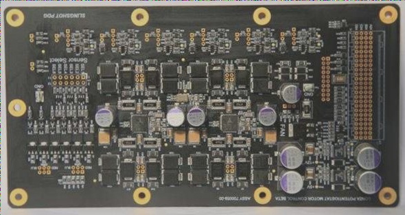
X-ray testing is a non-destructive method used to inspect the quality of soldering and assembly within a printed circuit board assembly (PCBA). This technology allows for the visualization of details such as solder joints, pads, component locations, and connectivity within the PCBA, enabling the detection of potential defects and issues.
- Soldering quality inspection: X-ray images can be used to assess the integrity of solder joints, the correct connection of pads to components, and the presence of issues such as bubbles, cracks, or cold soldering.
- Component position detection: X-ray imaging can verify the accurate placement of components on the PCBA and detect any misalignment or offset issues.
- Connectivity inspection: X-ray images help identify any issues with wire connections, such as short circuits, broken circuits, or misalignments.
- Hidden defects inspection: X-ray technology allows for the detection of hidden defects within the PCBA, such as air bubbles, foreign objects, and metal debris under soldering points.
X-ray testing plays a crucial role in the PCBA manufacturing process, enabling manufacturers to address potential issues promptly and improve product quality and reliability. Widely used in the electronics manufacturing industry, especially for high-density and complex PCBA inspection, this method provides comprehensive and accurate results. It is particularly valuable in sectors such as aerospace, communication, medical devices, and automotive electronics, delivering fast, precise, and reliable inspection outcomes to ensure the quality and reliability of PCBA.

