In recent years, the longevity of laser sources used in laser systems has significantly improved, with many now being virtually maintenance-free. In terms of production, laser systems typically operate at Class 1 safety levels, meaning they don’t require additional protective devices. The LPKF laser system, for instance, is equipped with an efficient dust collection system, ensuring no harmful substances are emitted during operation. Coupled with user-friendly software that simplifies control, laser technology is quickly replacing traditional mechanical processes, leading to significant cost savings by eliminating the need for specialized tooling.
When it comes to PCB cutting or splitting, a CO2 laser system with a wavelength of approximately 10.6 μm is a popular choice. This type of laser is cost-effective and can deliver power in the range of kilowatts. However, it does generate considerable heat during the cutting process, which often results in carbonization at the edges of the material.
In contrast, UV lasers, which operate at a wavelength of 355 nm, offer distinct advantages. These lasers are easier to focus optically, and when focused, the spot diameter can be as small as 20 μm with laser powers below 20 watts. The energy density generated by this process can rival that of the sun’s surface. UV lasers are particularly effective for cutting and marking rigid boards, rigid-flex boards, flexible boards, and their accessories.
What sets UV laser technology apart in PCB applications, particularly in the SMT industry and micro-drilling for PCB manufacturing, is its precision and technical advantages. The UV laser cutting system is capable of making precise cuts along the required contours, with multiple passes required depending on the thickness of the circuit board material. Thinner materials can be cut at faster speeds, while the laser pulse energy must be carefully calibrated to avoid damaging the material. If the laser pulse is insufficient to fully penetrate the material, only surface scratches will appear. This characteristic makes UV lasers ideal for marking 2D codes or barcodes for traceability in subsequent production stages.
In summary, UV laser technology offers excellent precision, minimal heat impact, and high versatility in PCB applications, making it a superior choice for many manufacturing processes.

The pulse energy of UV lasers acts on the material for just a few microseconds, producing minimal thermal effects on the area adjacent to the cut (within a few micrometers). As a result, there is no need to worry about heat-induced damage to the components. The lines and solder joints near the edges remain intact, and the cuts are clean, free of burrs. This precision ensures high-quality processing, especially when dealing with sensitive components.
Moreover, the LPKF UV laser system, which integrates CAM software, streamlines the entire process. It can directly import data from CAD files, allowing users to edit the laser cutting path, define the cutting contours, and select processing parameters that suit various materials. This seamless integration not only makes the system efficient for mass production but also adaptable for small-batch or prototype manufacturing.
Through holes are essential in circuit boards for connecting lines between the front and back of a double-sided board or interlayer lines in a multilayer board. To ensure electrical conductivity, these holes require a metal plating on their walls after drilling. However, traditional mechanical drilling methods struggle to meet the demands of smaller hole diameters. Despite increasing spindle speeds, the reduced radial speed of precision tools makes it difficult to achieve the desired results. Additionally, tool wear adds an economic burden.
Laser drilling provides a more effective solution, particularly for flexible circuit boards. During the drilling process, the laser can accurately define the micro-hole contour at the hole’s center, which offers greater precision than conventional methods. The system is capable of drilling micro-holes as small as 20μm in diameter on organic and non-organic substrates while maintaining a high diameter-to-depth ratio. This precision is critical for flexible circuit boards, IC substrates, and HDI boards, all of which require fine drilling capabilities.
In the manufacturing of electronic components, certain processes necessitate the cutting of prepreg materials. Prepreg, commonly used in multilayer circuit boards, helps bond the different layers together during the pressing process. However, depending on the circuit design, certain areas of the prepreg must be cut and opened prior to pressing. UV lasers can be used to form precise contours on these sensitive layers without causing any damage, which is especially beneficial when working with delicate materials.
A similar technique is applied to cover films in flexible printed circuits (FPC). These films are typically made from polyimide and a thin adhesive layer (25μm or 12.5μm thick). Due to their thin nature, cover films are prone to deformation under mechanical stress, making non-contact laser processing the ideal solution. The laser offers a precise and clean cut without applying stress to the material. Additionally, the use of a vacuum suction table ensures the material is held firmly in place and maintains its flatness during processing.
For rigid-flex boards, which combine rigid and flexible PCBs, laser depth cutting is used to separate the flexible section from the rigid portion. During the pressing process, the flexible PCB is not bonded to the rigid layer, and the rigid cover that overlays the flexible part is removed via laser cutting. This method is also ideal for creating blind grooves, which are essential for embedding integrated components on multilayer boards. The UV laser can accurately cut these blind grooves, ensuring precise separation without compromising the integrity of the multilayer structure.
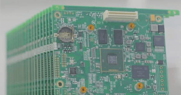
In the final stages of PCB manufacturing, especially after surface-mount technology (SMT) assembly, the circuit board is often cut into smaller sub-boards. This process requires careful consideration of the method used for splitting. Traditional methods, such as mechanical cutting, stamping, and contour milling, are suitable for most PCBs. However, for more complex circuits, thin substrates, or materials sensitive to mechanical stress, UV laser cutting is the superior choice. It provides high precision, minimizes dust generation, and reduces dimensional deviation, making it especially advantageous for delicate boards.
The UV laser’s short wavelength allows it to effectively process a wide range of materials, making it particularly suitable for the electronics industry. Beyond PCB cutting and drilling, UV lasers can also be used for LTCC component processing, including cutting, direct writing, and drilling—all in a single operation. Laser cutting or drilling in the PCB industry requires only a few watts, typically more than ten watts, of UV laser power, which is much lower than the kilowatt-level power required for other laser types.
With the increasing demand for flexible circuit boards in industries like consumer electronics, automotive manufacturing, and robotics, UV laser technology has become a top choice. Its flexibility, high precision, and controllable processing capabilities make it indispensable for drilling and cutting thin, flexible PCBs and other sensitive materials.
When it comes to PCB cutting or splitting, a CO2 laser system with a wavelength of approximately 10.6 μm is a popular choice. This type of laser is cost-effective and can deliver power in the range of kilowatts. However, it does generate considerable heat during the cutting process, which often results in carbonization at the edges of the material.
In contrast, UV lasers, which operate at a wavelength of 355 nm, offer distinct advantages. These lasers are easier to focus optically, and when focused, the spot diameter can be as small as 20 μm with laser powers below 20 watts. The energy density generated by this process can rival that of the sun’s surface. UV lasers are particularly effective for cutting and marking rigid boards, rigid-flex boards, flexible boards, and their accessories.
What sets UV laser technology apart in PCB applications, particularly in the SMT industry and micro-drilling for PCB manufacturing, is its precision and technical advantages. The UV laser cutting system is capable of making precise cuts along the required contours, with multiple passes required depending on the thickness of the circuit board material. Thinner materials can be cut at faster speeds, while the laser pulse energy must be carefully calibrated to avoid damaging the material. If the laser pulse is insufficient to fully penetrate the material, only surface scratches will appear. This characteristic makes UV lasers ideal for marking 2D codes or barcodes for traceability in subsequent production stages.
In summary, UV laser technology offers excellent precision, minimal heat impact, and high versatility in PCB applications, making it a superior choice for many manufacturing processes.
The pulse energy of UV lasers acts on the material for just a few microseconds, producing minimal thermal effects on the area adjacent to the cut (within a few micrometers). As a result, there is no need to worry about heat-induced damage to the components. The lines and solder joints near the edges remain intact, and the cuts are clean, free of burrs. This precision ensures high-quality processing, especially when dealing with sensitive components.
Moreover, the LPKF UV laser system, which integrates CAM software, streamlines the entire process. It can directly import data from CAD files, allowing users to edit the laser cutting path, define the cutting contours, and select processing parameters that suit various materials. This seamless integration not only makes the system efficient for mass production but also adaptable for small-batch or prototype manufacturing.
Through holes are essential in circuit boards for connecting lines between the front and back of a double-sided board or interlayer lines in a multilayer board. To ensure electrical conductivity, these holes require a metal plating on their walls after drilling. However, traditional mechanical drilling methods struggle to meet the demands of smaller hole diameters. Despite increasing spindle speeds, the reduced radial speed of precision tools makes it difficult to achieve the desired results. Additionally, tool wear adds an economic burden.
Laser drilling provides a more effective solution, particularly for flexible circuit boards. During the drilling process, the laser can accurately define the micro-hole contour at the hole’s center, which offers greater precision than conventional methods. The system is capable of drilling micro-holes as small as 20μm in diameter on organic and non-organic substrates while maintaining a high diameter-to-depth ratio. This precision is critical for flexible circuit boards, IC substrates, and HDI boards, all of which require fine drilling capabilities.
In the manufacturing of electronic components, certain processes necessitate the cutting of prepreg materials. Prepreg, commonly used in multilayer circuit boards, helps bond the different layers together during the pressing process. However, depending on the circuit design, certain areas of the prepreg must be cut and opened prior to pressing. UV lasers can be used to form precise contours on these sensitive layers without causing any damage, which is especially beneficial when working with delicate materials.
A similar technique is applied to cover films in flexible printed circuits (FPC). These films are typically made from polyimide and a thin adhesive layer (25μm or 12.5μm thick). Due to their thin nature, cover films are prone to deformation under mechanical stress, making non-contact laser processing the ideal solution. The laser offers a precise and clean cut without applying stress to the material. Additionally, the use of a vacuum suction table ensures the material is held firmly in place and maintains its flatness during processing.
For rigid-flex boards, which combine rigid and flexible PCBs, laser depth cutting is used to separate the flexible section from the rigid portion. During the pressing process, the flexible PCB is not bonded to the rigid layer, and the rigid cover that overlays the flexible part is removed via laser cutting. This method is also ideal for creating blind grooves, which are essential for embedding integrated components on multilayer boards. The UV laser can accurately cut these blind grooves, ensuring precise separation without compromising the integrity of the multilayer structure.
In the final stages of PCB manufacturing, especially after surface-mount technology (SMT) assembly, the circuit board is often cut into smaller sub-boards. This process requires careful consideration of the method used for splitting. Traditional methods, such as mechanical cutting, stamping, and contour milling, are suitable for most PCBs. However, for more complex circuits, thin substrates, or materials sensitive to mechanical stress, UV laser cutting is the superior choice. It provides high precision, minimizes dust generation, and reduces dimensional deviation, making it especially advantageous for delicate boards.
The UV laser’s short wavelength allows it to effectively process a wide range of materials, making it particularly suitable for the electronics industry. Beyond PCB cutting and drilling, UV lasers can also be used for LTCC component processing, including cutting, direct writing, and drilling—all in a single operation. Laser cutting or drilling in the PCB industry requires only a few watts, typically more than ten watts, of UV laser power, which is much lower than the kilowatt-level power required for other laser types.
With the increasing demand for flexible circuit boards in industries like consumer electronics, automotive manufacturing, and robotics, UV laser technology has become a top choice. Its flexibility, high precision, and controllable processing capabilities make it indispensable for drilling and cutting thin, flexible PCBs and other sensitive materials.