Challenges and Solutions in Flexible Circuit Design and Rigid PCB Design
- Understanding the unique requirements of flexible circuits is essential for PCB designers to create reliable solutions that balance electrical and mechanical functions.
- Avoid stress concentration in flexible circuits by maintaining a consistent circuit structure in bending areas and using proper conductor routing.
- Bending Ratio: Evaluate the minimum bending ratio to ensure the circuit can withstand bending without damage.
- Optimal Bending Ratio: Ensuring the circuit’s longevity and performance by using the optimal bending ratio.
- Conductor Routing: Proper conductor orientation and bending techniques can extend the circuit’s service life.
Conductor Placement and Design Tips:
- Place small conductors inside the bending area to prevent tension and avoid stacking conductors in multilayer structures.
- Flexible Circuit Conductor: The production process and considerations for designing flexible circuit conductors.
- Consider side etching effects when using thick copper foils and optimize conductor width for better etching results.
- Land Fillet: Adding fillets at conductor entry points can reduce stress concentration.
It is crucial to follow these guidelines to create durable and efficient flexible circuit solutions that meet both electrical and mechanical requirements.
Avoid Copper Tear-Stop Blocks
Avoid relying on copper tear-stop blocks to prevent tearing, as studies have shown they are ineffective in stopping tears or preventing cracks from spreading.
Design Solutions for Reducing Tearing
To reduce tearing, consider optimizing design elements such as conductor layout, copper thickness, and pad sizes to minimize stress during bending and flexing.
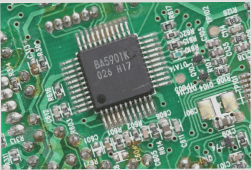
Vias for PCB Connection
Vias are essential for connecting multiple layers on a PCB. Blind vias connect outer layers to adjacent internal layers without passing through the entire circuit, while buried vias connect inner layers without extending to the outer layer. Both types increase manufacturing costs but provide more usable space on undrilled layers.
SMT Clearance Openings
- For SMT clearance openings, the common cover materials are polyimide film and flexible solder mask.
- Clearance openings in polyimide film can be created through drilling, milling, or punching, with resulting openings typically circular or elliptical.
- Flexible solder masks, like traditional PCB solder masks, are created using photosensitive imaging, allowing for openings of any shape.
Controlled Impedance and Signal Integrity
As electronic equipment speeds increase, ensuring the characteristic impedance of all components in an electronic assembly matches is crucial. Impedance mismatches lead to signal reflections and degradation, potentially causing equipment malfunction.
If you have any questions about PCBs, please contact us at info@wellcircuits.com.