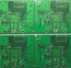
Common drilling holes in PCB circuit boards include through holes, blind holes, and buried holes. These three types of holes have distinct meanings and characteristics.
Via (VIA) refers to a common hole used to create electrical connections between copper traces on different layers of the circuit board. For example, blind and buried holes are types of vias, but they do not accommodate component leads or copper-plated holes for other reinforcement materials. Since PCBs are constructed by stacking multiple layers of copper foil, each layer is separated by an insulating layer, preventing direct communication between the copper layers. The via hole serves as the link that allows signal flow between these layers. This is why vias are sometimes referred to as “Chinese vias.”
The key characteristic is that to meet customer requirements, the through holes of the PCB must be filled. In the process of replacing the traditional aluminum plug hole method, a white mesh is used to complete both the solder mask and plug holes on the PCB, ensuring stable production, reliable quality, and improved performance. Vias primarily function to interconnect and conduct circuits. As the electronics industry rapidly advances, higher demands are placed on both the manufacturing processes and surface mount technologies for printed circuit boards. When applying the via hole plugging process, the following criteria must be met:

1. Copper is present in the via hole, and the solder mask may either be plugged or left unpluggd.
2. The through hole must contain both tin and lead, and there is a required thickness (4µm) to prevent solder mask ink from entering the hole, which could lead to hidden tin beads inside the hole.
3. Through holes must have solder mask ink plugs that are opaque, and there should be no tin rings, tin beads, or flatness issues.
**Blind Hole:** A blind hole connects the outermost layer of the PCB with the adjacent inner layer through an electroplated hole. Since the opposite side of the hole is not visible, it is referred to as a blind via. Blind vias are typically used to maximize space utilization between PCB circuit layers. In this case, the via hole reaches only one side of the printed board.
**Features:** Blind vias are located on the top and bottom surfaces of the PCB with a certain depth and are used to connect the surface circuit with the inner circuit below. The depth of the hole generally does not exceed a specific ratio relative to the hole diameter. This method requires careful control of the drilling depth (Z-axis) to avoid complications in electroplating. Due to the complexity of the process, few manufacturers use this method. Alternatively, the necessary circuit layers can be pre-arranged, and the vias drilled before the layers are bonded together, though this requires more precise alignment equipment.
**Buried Via:** A buried via links any internal circuit layers within the PCB but does not connect to the outer layers. These vias are holes that do not extend to the surface of the PCB.
**Features:** The buried via process cannot be performed after bonding; it must be drilled within the individual circuit layers before bonding. The inner layers are partially bonded and then electroplated before the full bonding process. This method ensures better conductivity compared to blind holes. However, the process is more time-consuming, making it the most expensive. Buried vias are typically used in high-density circuit boards to optimize the usable space of other circuit layers.
Drilling is a crucial step in the PCB production process and must be done with care. Drilling creates the necessary via holes in the copper-clad board to provide electrical connections and secure the components. Improper drilling can lead to issues with the via holes, preventing proper component placement and causing the board to become unusable. In extreme cases, this could result in the entire board being scrapped, making the drilling process highly critical.
If your have any questions about PCB ,please contact me info@wellcircuits.com
Via (VIA) refers to a common hole used to create electrical connections between copper traces on different layers of the circuit board. For example, blind and buried holes are types of vias, but they do not accommodate component leads or copper-plated holes for other reinforcement materials. Since PCBs are constructed by stacking multiple layers of copper foil, each layer is separated by an insulating layer, preventing direct communication between the copper layers. The via hole serves as the link that allows signal flow between these layers. This is why vias are sometimes referred to as “Chinese vias.”
The key characteristic is that to meet customer requirements, the through holes of the PCB must be filled. In the process of replacing the traditional aluminum plug hole method, a white mesh is used to complete both the solder mask and plug holes on the PCB, ensuring stable production, reliable quality, and improved performance. Vias primarily function to interconnect and conduct circuits. As the electronics industry rapidly advances, higher demands are placed on both the manufacturing processes and surface mount technologies for printed circuit boards. When applying the via hole plugging process, the following criteria must be met:

1. Copper is present in the via hole, and the solder mask may either be plugged or left unpluggd.
2. The through hole must contain both tin and lead, and there is a required thickness (4µm) to prevent solder mask ink from entering the hole, which could lead to hidden tin beads inside the hole.
3. Through holes must have solder mask ink plugs that are opaque, and there should be no tin rings, tin beads, or flatness issues.
**Blind Hole:** A blind hole connects the outermost layer of the PCB with the adjacent inner layer through an electroplated hole. Since the opposite side of the hole is not visible, it is referred to as a blind via. Blind vias are typically used to maximize space utilization between PCB circuit layers. In this case, the via hole reaches only one side of the printed board.
**Features:** Blind vias are located on the top and bottom surfaces of the PCB with a certain depth and are used to connect the surface circuit with the inner circuit below. The depth of the hole generally does not exceed a specific ratio relative to the hole diameter. This method requires careful control of the drilling depth (Z-axis) to avoid complications in electroplating. Due to the complexity of the process, few manufacturers use this method. Alternatively, the necessary circuit layers can be pre-arranged, and the vias drilled before the layers are bonded together, though this requires more precise alignment equipment.
**Buried Via:** A buried via links any internal circuit layers within the PCB but does not connect to the outer layers. These vias are holes that do not extend to the surface of the PCB.
**Features:** The buried via process cannot be performed after bonding; it must be drilled within the individual circuit layers before bonding. The inner layers are partially bonded and then electroplated before the full bonding process. This method ensures better conductivity compared to blind holes. However, the process is more time-consuming, making it the most expensive. Buried vias are typically used in high-density circuit boards to optimize the usable space of other circuit layers.
Drilling is a crucial step in the PCB production process and must be done with care. Drilling creates the necessary via holes in the copper-clad board to provide electrical connections and secure the components. Improper drilling can lead to issues with the via holes, preventing proper component placement and causing the board to become unusable. In extreme cases, this could result in the entire board being scrapped, making the drilling process highly critical.
If your have any questions about PCB ,please contact me info@wellcircuits.com


