Benefits of Embedded Resistor and Capacitor Technology in PCBs
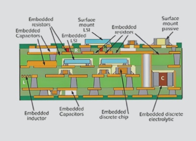
- Space-saving: Embedding resistors and capacitors within the internal layers of the PCB saves valuable surface space, resulting in a more compact design.
- Reduced circuit noise: Minimizes electromagnetic interference and noise, enhancing circuit stability and resistance to external interference.
- Improved signal integrity: Reduces signal transmission delays and reflection losses, improving signal integrity and reliability.
- Thinner PCB: Integration of components into internal layers allows for a thinner and lighter PCB, offering a streamlined design.
The embedded resistor and capacitor process, while advantageous, can be complex to manufacture and maintain due to limited accessibility and higher production costs for high-end electronic products.
In high-density circuit designs, this technology is particularly beneficial as it addresses issues related to PCB footprint, noise, and interference that surface-mounted components may introduce.
Steps in PCB Embedded Resistor and Capacitor Process:
- Internal Layer Fabrication: Specialized internal layers are created during PCB production to accommodate embedded components, utilizing techniques like plating and etching.
- Resistor/Capacitor Package: Components are packaged in specialized forms for integration within the PCB’s internal layers, designed to match thickness and provide good thermal conductivity.
- Embedding Resistors/Capacitors: Components are embedded into internal layers using compression methods or laser technology to etch voids and fill them with resistors and capacitors.
- Connection Layers: Integrated layers are connected to standard layers using conventional methods like lamination and drilling.
Advanced Integration Technology in PCBs: Embedded Resistors and Capacitors
Embedded resistor and capacitor process is an innovative technology that involves integrating resistors and capacitors within a PCB’s internal layers. This cutting-edge approach not only saves space but also reduces noise, enhances signal integrity, and results in a thinner and lighter PCB.
Despite its numerous benefits, it is essential to note that the manufacturing and maintenance of PCBs with embedded resistors and capacitors can be complex. Additionally, the higher cost associated with this process means that it is primarily utilized in high-end electronic devices that require top-notch performance.
If you have any inquiries regarding PCBs or PCBA, please do not hesitate to reach out to us at info@wellcircuits.com.


