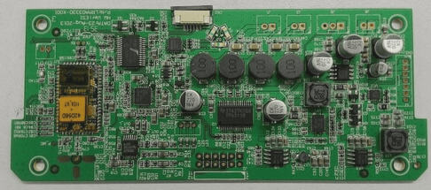
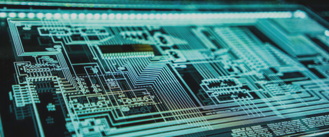
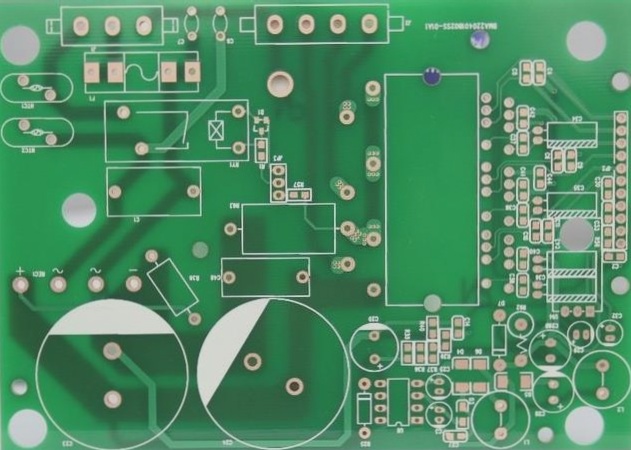
1. PCB board, also known as printed circuit board (Printed Circuit Board), can facilitate the connection of circuits and the realization of functions between electronic components. It is also a crucial component in power circuit design. In this article, we will be introducing the fundamental rules of PCB board layout and wiring.

1. Basic Rules of Component Layout
1) When laying out components, it is important to consider the circuit module. Components that realize the same function should be grouped together as modules. It is recommended to concentrate components within the same module, and ensure digital and analog circuits are separated.
2) Avoid mounting components and devices within 1.27mm of non-mounting holes such as positioning holes and standard holes. For mounting holes such as screws, keep a distance of 3.5mm (for M2.5) and 4mm (for M3) to prevent interference.
3) Do not place vias under horizontally mounted resistors, inductors (plug-ins), and electrolytic capacitors to prevent short circuits after wave soldering.
4) Maintain a distance of 5mm between the outside of the component and the edge of the board.
5) Ensure the distance between the outer side of the mounted component pad and the adjacent mounted component is greater than 2mm.
6) Metal shell components and metal parts should not touch other components or be close to printed lines and pads, with a spacing of at least 2mm. Positioning holes, fastener installation holes, elliptical holes and square holes should be at least 3mm from the edge of the board.
7) Heating elements should be evenly distributed and kept away from wires and other thermal elements.
8) Power sockets should be arranged around the printed board, and the bus bar terminals connected to the power socket should be on the same side. Power sockets and soldered connectors should not be placed between connectors for easier soldering and cable design. Consider the spacing of power sockets and welding connectors for easy insertion and removal of power plugs.
9) IC components should be unilaterally aligned, and polar components should be clearly marked with polarities. There should not be more than two directions for polarity markings on the same printed board, and if there are, the two directions should be perpendicular to each other.
10) Ensure proper density of wiring on the board, and fill areas with large differences in density with mesh copper foil with a mesh size over 8mil (or 0.2mm).
11) Avoid through-holes on patch pads to prevent loss of solder paste and ensure important signal lines do not pass between socket pins.
12) Patch components should be aligned on one side, with consistent character and packaging directions.
13) For devices with polarity, ensure the direction of polarity marking on the same board is as consistent as possible.
2. Component Wiring Rules
1) Avoid wiring in areas within 1mm of the edge of the PCB board and around mounting holes.
2) Power lines should be at least 18mil wide, signal lines should be at least 12mil wide, and CPU input and output lines should be at least 10mil (or 8mil) wide. The line spacing should not be less than 10mil.
3) The normal via hole should be at least 30mil.
4) Dual in-line, 1/4W resistance, and electrodeless capacitor pad and aperture sizes should follow the specified dimensions.
5) Ensure power and ground wires are radial, and avoid looping signal wires.
3. Improving Anti-Interference Ability and Electromagnetic Compatibility
When developing electronic products with processors, it is important to consider the following to improve anti-interference ability and electromagnetic compatibility:
3.1 Specific systems that require attention to anti-electromagnetic interference:
1) Systems with high microcontroller clock frequency and fast bus cycle.
2) Systems containing high-power, high-current drive circuits.
3) Systems with weak analog signal circuits and high A/D conversion circuits.
3.2 Measures to increase anti-electromagnetic interference capability:
1) Select microcontrollers with lower external clock frequencies to reduce noise and improve anti-interference ability.
2) Reduce distortion in signal transmission to prevent signal reflection and impedance problems.
3) Minimize cross-interference between signal lines by separating high-speed digital circuits and noise sources.
4) Reduce noise from the power supply and ensure sensitive circuits are shielded from interference.
5) Consider the high-frequency characteristics of printed circuit boards and components, and ensure proper layout partitioning.
6) Grounding is crucial for overcoming electromagnetic interference, so single-point grounding and careful ground wire layout are essential.
7) Make use of decoupling capacitors to remove high-frequency components and bypass high-frequency noise from devices.
3. Experience in Reducing Noise and Electromagnetic Interference
1) Consider using low-speed chips instead of high-speed chips where applicable.
2) Connect resistors in series to reduce the transition rate of control circuits.
3) Provide damping for relays and similar devices.
4) Use a frequency clock that meets system requirements.
5) Keep the clock generator close to the device using the clock, with proper grounding.
6) Ensure proper grounding of I/O drive circuits, and filter noise from high-noise areas.
7) Connect unused ends of MCD to high, grounded, or defined as output end.
8) Do not leave input terminals of unused gate circuits floating, and connect unused operational amplifier terminals as advised.
9) Use 45° fold lines instead of 90° fold lines to reduce external emission and coupling of high-frequency signals.
10) Divide the printed board according to frequency and current switching characteristics, and maintain proper separation between noise and non-noise components.
11) Ensure single-point connection to the power supply and single-point grounding, with thick power and ground lines.
12) Keep clocks, buses, and chip select signals away from I/O lines and connectors.
13) Keep analog voltage input lines away from digital circuit signal lines, especially the clock.
14) Ensure the digital part and analog part of A/D devices are unified rather than crossed.
15) Minimize interference by keeping component pins and decoupling capacitor pins short.
16) Use thick key lines and add protective ground on both sides, with short and straight high-speed lines.
17) Avoid running sensitive lines in parallel with high-current, high-speed switching lines.
18) Do not run traces under quartz crystals and under noise-sensitive devices.
19) Avoid forming current loops around low-frequency circuits.
20) Avoid forming signal loops, and keep them as small as possible.
21) Add one decoupling capacitor per IC, and consider adding small high-frequency bypass capacitors.
22) Use large-capacity tantalum capacitors or polycarbonate capacitors instead of electrolytic capacitors, with proper grounding.


