The Advantages of True-Color LCD Displays in PCB Embedded Systems
With the rapid advancements in display technology, true-color LCD displays are becoming increasingly crucial in PCB embedded systems. These displays offer high resolution, excellent contrast, and clarity, making them highly desirable for various applications.
Challenges with Implementing LCD Controllers on PCBs
When it comes to integrating LCD controllers on PCBs, two primary approaches are commonly used: ARM-based embedded controllers and standalone control devices. However, both methods have their limitations. Embedded controllers can strain the PCB processor and limit display frame rates, while external control devices tend to be costly and less versatile.
Proposed Solution: ARM and FPGA-Based LCD Controller
To address these challenges, a design scheme combining ARM and FPGA for the LCD controller is proposed. This innovative approach aims to enhance video memory writing speeds, reduce processor load, and improve overall performance by leveraging the Framebuffer device in the LINUX OS environment.
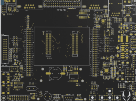
Key Components and Operational Flow
- Microcontroller
- FPGA (LCD controller)
- Storage unit
- Peripheral interface
The system operates by retrieving display data from the microcontroller, storing it in the display buffer SRAM, and presenting real-time data on the LCD display through a data format conversion circuit. The FPGA, specifically Altera’s Cvclone series EPlC6Q240, plays a crucial role in ensuring high-speed data transmission and precise control timing.
Optimizing Performance
To achieve efficient performance, the system utilizes a 512 KB IS61LV51216AL SRAM module with rapid read and write speeds. The main control unit, powered by ATMEL’s AT91RM9200, operates as the system’s MCU, running on the ARM920T core at 180 MHz. The system’s software architecture is divided into FPGA-based LCD controller design and Framebuffer driver design under LINUX OS, enhancing data processing and display performance.
Enhancing Display Control
The FPGA employs an internal phase-locked loop IP module to generate essential control signals such as the pixel clock signal, line/field synchronization signal, and enable signal. By utilizing Verilog hardware description language and state machine methodology, the timing control module ensures precise control signal generation, meeting the LCD’s timing requirements.
Efficient Data Transmission
To manage data transmission between different clock domains, an FPGA-designed asynchronous FIFO is employed, synchronizing data under ARM clock control and pixel clock signal control for optimal performance.