Using Labels in KiCad for Component Connections
To create circuits efficiently in KiCad, there are four primary methods for connecting components:
- Connecting via Tracks (Lines)
- Connecting with Net Labels
- Connecting with Hierarchical Labels
- Connecting with Global Labels
Connecting via Tracks (Lines)
Connecting components using tracks or lines is a common method in KiCad. It’s important to avoid inadvertent connections while moving the lines around. See Image 1 below for an example:
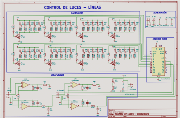
Image 1. Component connection via tracks (lines).
It’s crucial to double-check designs to prevent errors like overlapping lines without proper connections, as shown in Image 2:
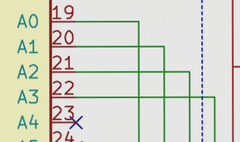
Image 2. Overlapping lines without proper connection.
Always ensure that connections are properly made to avoid unintended connections, as shown in Image 3:
Image 3. Error in track connection.
For clearer design organization, different functional blocks can be distinguished using colored lines, such as Power Supply Stage, Comparator/Amplifier Stage, Arduino Nano Stage, and Lighting Stage.
To connect components via tracks, use the Track option in KiCad and drag the cursor from one component to another.
Connecting with Net Labels
Using net labels in KiCad reduces the number of tracks needed between components and enhances visual clarity in circuit design. Image 5 demonstrates the same components connected with net labels:
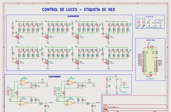
Image 5. Connection via net labels.
Net labels, as shown in Image 6, help establish connections between components without the need for continuous tracks:
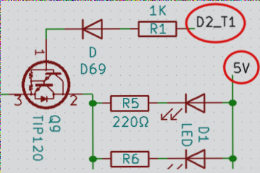
Image 6. Net label for the Lighting stage.
Creating Net Labels for PCB Connections
When working on PCB design, ensuring accurate connections is crucial. One way to achieve this is by using net labels. Here’s a step-by-step guide on how to create net labels for your PCB connections:
1. Selecting the Net Label Icon
To begin, select the net label icon from the toolbar used for track connections. This icon is essential for creating net labels accurately.
2. Creating the Label
Click on the point where you want to create the label. A text window will appear, allowing you to enter a name to identify the connection.
3. Copying and Pasting
After entering the label name, select it, copy it, and press accept. This step helps minimize transcription errors and ensures the correct label is copied.
4. Completing the Connection
Move to the other connection point, click, paste the copied label name, and press Accept to complete the connection. Repeat this process for all your connections using net labels.
By following these steps, you can effectively create and manage net labels for your PCB connections, aiding in a seamless design process.