Ensuring Quality in PCB Manufacturing: Defect Detection and Inspection
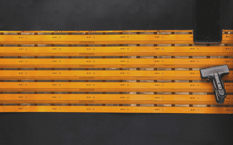
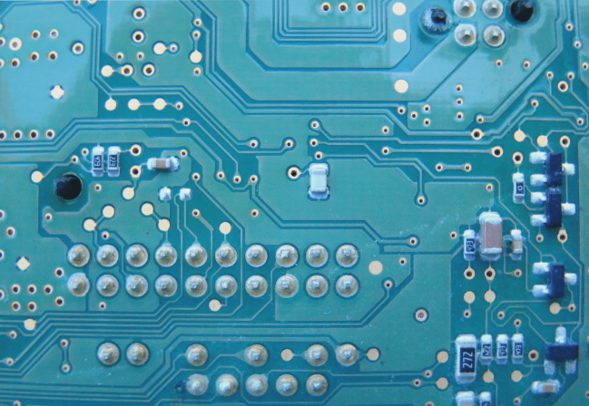
In the competitive electronic products market, PCB manufacturers prioritize product quality by monitoring semi-finished and finished products for defects throughout the manufacturing process. Common defects in assembled and soldered printed circuit boards include missing components, soldering issues, component failures, and more.
Testing Equipment for PCB Quality Assurance
- Automatic Optical Inspection (AOI) systems assess inner layers pre-lamination.
- X-ray systems monitor alignment and detect defects post-lamination.
- Scanning laser systems inspect pad layers before reflow.
These technologies, combined with intuitive inspection integration and automatic component checks, ensure reliable final assembly and soldering. Despite these measures, a thorough final inspection of assembled PCBs remains essential for product and process evaluation.

Manual vs. Automated Inspection
Final inspections can be manual or automated, with both methods often used together. Manual inspection involves visual assessment by an operator, while automated systems use computer-aided analysis to detect defects. X-ray, ultrasonic, optical, laser, and infrared technologies offer various inspection methods to assess solder joints and detect defects.
Integration for Comprehensive Defect Detection
Automated inspection technologies complement manual methods, especially for specialized applications. Integrating X-ray and manual optical inspection is a highly effective strategy for detecting defects in assembled boards.
If you require PCB manufacturing services, feel free to contact us for assistance.