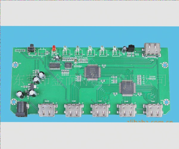
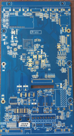
Essential Tips for PCB Circuit Board Design
- The importance of defining processing levels: To avoid challenges in soldering components, clearly define the distinctions between the positive and negative sides of a single-sided board.
- Maintain a minimum distance between large copper areas and the outer frame: A distance of 0.2mm is crucial to prevent copper warping during the milling process, which can lead to issues like flux drop.
- Consider filler blocks for drawing pads: While filler blocks can be checked during PCB design, they may complicate the soldering process and hinder the generation of solder mask data.
- Isolate connections on the electrical ground layer: Carefully isolate multiple power supply or ground groups to prevent short-circuiting and block connection areas on the printed board.
- Ensure proper placement of characters: Avoid hindering testing and soldering by correctly sizing and placing characters on SMD soldering pads.
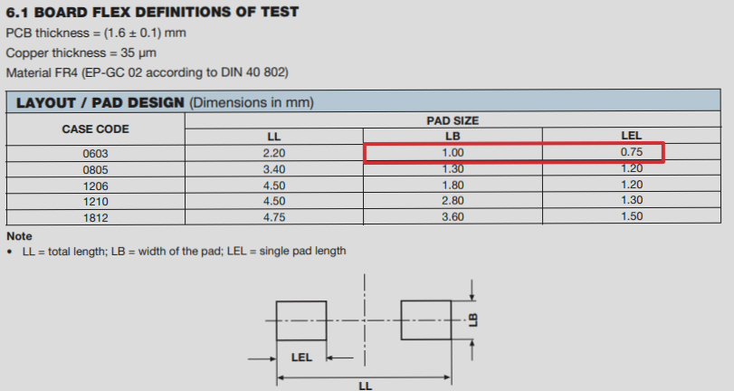
- Check surface mount device pad length: Adequate pad length is essential for continuity testing, especially for densely packed devices with minimal pin spacing.
- Set pad aperture for single-sided pads: If drilling is required, set the aperture to zero to prevent issues during drilling data generation.
- Avoid pad stacking issues: Be cautious of stacked holes that can lead to drill bit breakage and consider drawing negative film as an isolation disk in multi-layer boards to prevent scrap.
Understanding these intricacies in PCB circuit board design is crucial to ensure the efficient functioning of electronic devices across various industries.