Introduction:
When current flows through a circuit, the high-speed signals established will follow the path of least impedance rather than least resistance. Return path is the path the current takes to return to the source. We will discuss which return path can be used to make our PCB designs better.
Over time the demand for smaller PCBs has increased rapidly. At the same time the use of flexible and rigid-flex circuits also increased. As a result the operating voltages have reduced dramatically. But engineers always aim to make their designs better, faster and more accurate. How can you achieve that?
Routing Return Paths
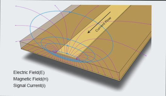
We know that an electric field is set up in the areas an alternating current passes through in the circuit. These field lines will permeate through the surrounding conductors and transfer to nearby circuits too. The time taken for the changes in magnetic field to reach the far ends of your circuit is actually at a fraction of the speed of light.
Whenever a change of state (high/low logic) occurs, an electric potential is established and a current passes through the circuit. The electric field in turn generates a magnetic field around the conductor the current flows through. The changes in magnetic field will take time to propagate and therefore the two ends of a trace in the PCB may be in two different states.
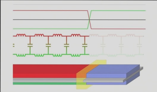
In this state a return path for the current will be formed by the inductive and capacitive coupling. If an immediate return path is not provided, unwanted currents may establish in nearby conductors. Always remember to provide a ground return path in the same layer (or adjacent layer) for single-ended signals, power planes and differential pairs.
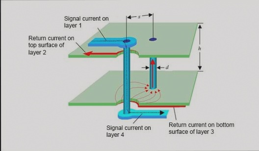
The Path of Least Impedance for high-speed signals
High speed signals, as mentioned before will follow the path of least impedance. Engineers sometimes forget about the impedance and focus on the resistive part of return paths. Remember in return paths the reactive part of impedance becomes more important as the frequency is increased and the rise/fall time decreases. In some cases the return path of the current will flow directly underneath the conductor. Therefore you should provide a desirable path before a less desirable path is established in your circuit.
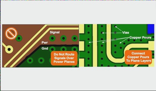
At low frequency the return path will flow directly from the load back to source. As the frequency is increased a low-impedance path is created by the mutual inductance between the trace and copper beneath it. As a result the return current in the ground place will follow the trace on the signal layer.
Using Return Paths in PCB Design
Route the fast-changing signals with an immediate return path in the surrounding area. Make sure the differential traces coming out of the package pins are immediately brought into close proximity. Clock signals should be surrounded by ground pours and have an uninterrupted ground place beneath them to reduce the radiated EMI noise. If your device undergoes FCC testing then you will have to route your fast-changing signals between two ground planes and use via-stitching to surround them.
Two key ways to reduce ground noise in PCB layout are to:
1: Keep differential pairs together through their entire route in PCB
2: Provide a ground return path either directly beneath or directly adjacent to your signal lines in the PCB.
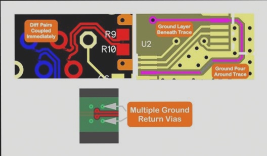
Usually signals that travel over the power planes before reaching the ground layers share their electric fields with the power place and can as a result create noise in the signal lines.
Conclusion:
In order to reduce unwanted currents from forming in your circuit, it is important to create a proper return path carefully planned out. You should provide ground return vias and paths for all the high speed signals passing through the circuit.


