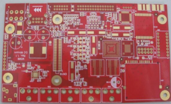
1. When wiring PCBs, it’s common for a trace to pass through a restricted area where space limitations necessitate the use of a thinner line.
2. Once the trace exits this area, it returns to its original width.
3. Variations in trace width can lead to changes in impedance, resulting in reflections that can impact the signal quality.
4. So, under what conditions can we disregard this effect, and when must we account for its implications?
5. There are three factors associated with this phenomenon: the extent of impedance change, the rise time of the signal, and the delay introduced by the narrower line.
6. Let’s first examine the extent of the impedance change.
7. Many circuit designs require that reflected noise remains below 5% of the voltage swing, which ties back to the noise budget of the signal.
8. Using the reflection coefficient formula, we can approximate the rate of impedance change as: △Z/Z1 ≤ 10%.
9. As you may know, the typical impedance tolerance on circuit boards is ±10%, which is the underlying issue.
1. If the PCB impedance changes only once, for instance, when the line width is altered from 8 mils to 6 mils and the 6 mil width is maintained, the noise budget requirement stipulates that the signal reflection noise at this sudden change must not exceed 5% of the voltage swing. Consequently, the impedance change must be kept under 10%. Achieving this can sometimes be challenging. Taking a microstrip line on an FR4 board as an example, let’s perform a calculation. When the line width is 8 mils and the thickness from the line to the reference plane is 4 mils, the characteristic impedance is measured at 46.5 ohms. Upon changing the line width to 6 mils, the characteristic impedance shifts to 54.2 ohms, resulting in an impedance change rate of 20%. This causes the amplitude of the reflected signal to surpass the standard limits. The effect on the signal also depends on the signal rise time and the delay from the driving end to the reflection point. Nevertheless, this represents a potential issue. Fortunately, this challenge can be mitigated through impedance matching termination.
2. When the PCB impedance changes twice, for example, first reducing the line width from 8 mils to 6 mils and then reverting to 8 mils after extending 2 cm, reflections will occur at both ends of the 2 cm long, 6 mil wide line. If the impedance increases, positive reflection occurs; if it decreases, negative reflection results. If the interval between these two reflections is sufficiently short, they may cancel each other out, thus minimizing the impact. Assuming the transmission signal is 1V, a reflection of 0.2V occurs during the first regular reflection, with 1.2V continuing forward. In the second reflection, -0.2 * 1.2 = -0.24V is reflected back. If the length of the 6 mil line is extremely short and both reflections happen almost simultaneously, the total reflection voltage could be only 0.04V, which is below the 5% noise budget requirement. Therefore, whether this reflection affects the signal and the extent of that effect depends on the time delay during the impedance change and the signal rise time. Research and experiments indicate that as long as the time delay at the impedance change is less than 20% of the signal rise time, reflected signals will not pose issues. For example, if the signal rise time is 1 ns, then the time delay at the impedance change must be less than 0.2 ns, corresponding to about 1.2 inches, to avoid problems. In other words, for this scenario, as long as the length of the 6 mil wide trace is under 3 cm, there should be no issues.
3. When designing PCB traces with varying widths, it is crucial to analyze the specific circumstances carefully to determine whether an impact will occur. Three key parameters need attention: the magnitude of the impedance change, the signal rise time, and the length of the neck-shaped section resulting from the line width change. Estimate based on the aforementioned method, allowing for a reasonable margin. If feasible, try to minimize the length of the neck.
4. It is important to note that in practical PCB manufacturing, parameters may not align precisely with theoretical predictions. Theory serves as a guide for our designs, but it should not be rigidly applied. After all, this is a field grounded in practicality. Estimated values should be adjusted based on actual conditions before application in design. If you feel inexperienced, it’s wise to adopt a conservative approach initially, adjusting as needed based on manufacturing costs.
If you have any PCB manufacturing needs, please do not hesitate to contact me.Contact me