PCB Design Best Practices for Optimal Manufacturing
1. Line Width, Spacing, and Via Specifications
- Minimum Line Width: 6 mils (0.153 mm)
- Minimum Line Spacing: 6 mils (0.153 mm)
- Distance Between Trace and Outline: 0.508 mm (20 mils)
Designing PCBs with a minimum line width of 6 mils (0.153 mm) ensures manufacturability and reduces the risk of defects. For multilayer boards, consider setting the inner layer’s minimum line width at 8 mils for better results.
Ensure a minimum line spacing of 6 mils (0.153 mm) for optimal production reliability. Increasing line spacing to 10 mils is a common industry practice that enhances manufacturability.
Maintain a gap of at least 20 mils (0.508 mm) between the trace and the PCB outline to prevent edge-related defects during fabrication.
2. Via Specifications
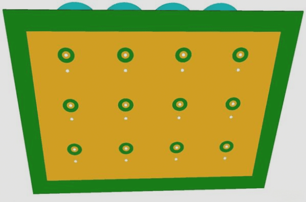
- Minimum Via Hole Diameter: 0.3 mm (12 mils)
- Pad Size for Vias:
Ensure via holes have a diameter of at least 0.3 mm (12 mils) to avoid manufacturing issues and ensure reliable connections.
Pad sizes for vias should not be smaller than 6 mils (0.153 mm) to support reliable connections. Consider increasing the pad size to 8 mils (0.2 mm) for improved reliability.
Key Takeaways
- Larger Design Features Enhance Manufacturability
- Design for Manufacturability
- Optimal Via Hole and Pad Design
Designing with larger line widths and spacings improves production yield and reduces defects.
Adhering to industry standards while considering increased values can boost success in PCB production.
Ensure via holes and pad dimensions meet requirements for reliable electrical connections.
Following these guidelines ensures your PCB is manufacturable, reliable, and of high quality, reducing risks during production.
Additional Considerations for PCB Design
1. Via Hole Spacing
Maintain a minimum spacing of 6 mils between via holes for reliable manufacturing and signal integrity.
2. Pad and Outline Spacing
Ensure a distance of at least 0.508 mm (20 mils) between PCB pads and outline lines to facilitate routing and prevent fabrication issues.
3. Through-Hole (PTH) Pad Design
- The through-hole pad size should exceed the component pin diameter by at least 0.2 mm for smooth component insertion.
- PTH pad outer rings should have a minimum width of 0.2 mm for mechanical reliability.
- Maintain a spacing of at least 0.3 mm between through-holes for optimal performance.
4. Anti-Soldering and SMD Window Requirements
PCB Design Guidelines for Efficient Manufacturing
- Window for Anti-Soldering
- Character Design
- Character width should be at least 0.153 mm.
- Character height should be at least 0.811 mm.
- Width-to-height ratio should ideally be 5:1.
- Non-Metalized Slot Hole Spacing
- Panelization (Imposition) Guidelines
- No-Gap Panelization: Boards are placed directly adjacent to each other.
- Gap Panelization: A gap of at least 1.6 mm is left between boards for easier separation post-manufacturing.
- V-Cutting Considerations
When designing areas near plug-in holes, ensure a minimum clearance of 0.1 mm on each side to prevent solder bridges and manufacturing errors, especially in single-sided Surface-Mount Device (SMD) windows.
Legible characters on the PCB are crucial for assembly and maintenance. Follow these specifications:
Poorly designed characters can lead to production difficulties and unclear labeling, impacting assembly and troubleshooting processes.
For non-metalized slot holes, maintain a minimum spacing of 1.6 mm to avoid milling complications, reduce production time, and ensure smoother processing for higher PCB quality.
Panelization involves arranging multiple PCBs on a single manufacturing panel, with two main types:
Smaller gaps can lead to milling difficulties and damage risks during separation. Optimal gap size is around 0.5 mm with a 5 mm process edge along the perimeter.
Ensure V-cut length exceeds 8 cm to prevent operational issues and keep V-cut width under 32 cm to fit into cutting machines. V-cuts must be made in straight lines, so consider board layout for feasibility.
Conclusion
Adhering to these PCB design guidelines is crucial for efficient manufacturing, meeting functional and quality standards. Clear pad designs, proper hole spacing, and attention to detail in features like characters and slot holes will reduce complexity and enhance overall PCB quality.