Enhancing PCB Assembly with Vector Imaging Technology
Advanced Graphic Location Search Method
- Vector imaging technology enhances accuracy, speed, and reliability in PCB assembly.
- Seamlessly integrated into dedicated production environments for PCBA OEM manufacturers and EMS providers.
- Focus on enhancing component inspection capabilities and reducing manufacturing costs.
New Vector Inspection Techniques
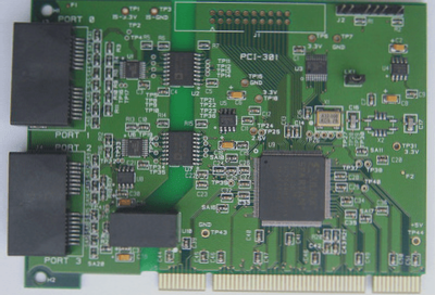
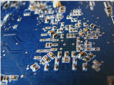
- Modern circuit boards require advanced inspection methods due to increased density and compact component packaging.
- Vector imaging technology in PCB assembly improves inspection accuracy, speed, and reliability.
Challenges in PCB Assembly
- Equipment performance varies based on specific requirements and technological advancements.
- Challenges include solder paste application, component placement, reflow soldering, and inspection.
Evolution of Inspection Methods
- X-ray, laser scanning, AOI, and hybrid X-ray/AOI inspection methods have been developed.
- AOI offers online inspection capabilities and can detect various component packages.
- Traditional AOI relies on gray-scale correlation for component identification.
Vector Imaging Technology Advantages
- Uses composite images and intersection vectors to define component shapes accurately.
- Relies on direction and inclination to represent components.
- Integrates SPC software, graphic libraries, and machine code conversion for optimal performance.
Optimizing Visual Effectiveness
- Utilizes multiple light sources to enhance contrast and imaging clarity.
- Requires component height to be less than 8mm for accurate recognition.
Advantages of Vector Imaging Technology in PCB Inspection
Vector imaging technology is a cutting-edge method used in PCB inspection that offers several advantages over traditional pixel grid systems. Unlike pixel-based methods, vector imaging technology relies on geometric information, ensuring consistent measurements and accurate analysis regardless of component rotation or changes in color, lighting, and background.
The Vector Imaging Inspection Process
- The system identifies and isolates main features on the component image map, measuring characteristics like shape, size, angle, radian, and brightness.
- Evaluates the spatial relationship between the composite image and the component’s main features.
- Calculates the x, y, and θ values on the circuit board, independent of component rotation or appearance changes.
One key advantage of vector imaging technology is its adaptability to different components on the circuit board as long as a reference model is available. This flexibility allows for seamless transition between visual inspection devices with varying optical systems, ensuring accurate analysis even when image sizes differ.
Furthermore, vector imaging technology can effectively handle alterations in PCB component appearance, including new features or obscured parts due to overlap. In contrast, traditional pixel grid systems may struggle to analyze obscured components accurately.