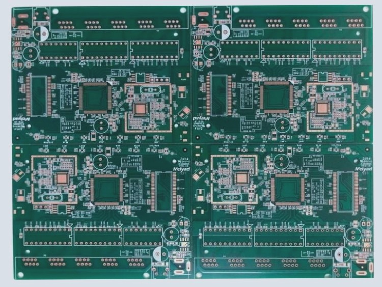
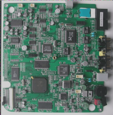
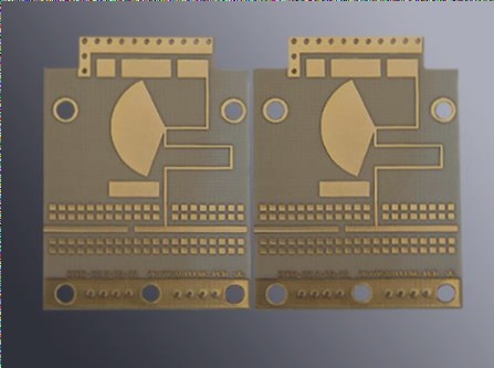
The process of manufacturing PCBs varies depending on their type. For instance, a flexible silver paste printed circuit board, commonly found in computer keyboards, employs a flexible insulating substrate with a silver-white conductive pattern applied via general screen printing methods. In contrast, the PCBs seen in Computer City, on computer motherboards, graphics cards, network cards, modems, sound cards, and household appliances, typically use substrates made from paper (commonly for single-sided boards) or glass cloth (preferred for double-sided and multilayer boards). These substrates are impregnated with phenolic or epoxy resins and laminated with copper-clad film on one or both sides before curing, resulting in what is known as a rigid board. When a conductive pattern is added to such boards, they are termed rigid printed circuit boards.
PCBs are categorized based on their structure: single-sided boards feature patterns on one side, while double-sided boards feature patterns on both sides interconnected through hole metallization. Multiple layers of interconnected conductive patterns, designed with alternating insulating bonding materials, constitute multilayer printed circuit boards, which can range from four to over a hundred layers depending on application complexity.
The production process of PCBA involves a multitude of intricate steps, spanning from mechanical and chemical processing to photochemical, electrochemical, and thermochemical processes, often aided by computer-aided design (CAD) and computer-aided manufacturing (CAM). Despite advancements, challenges persist, with intermittent issues arising throughout the assembly line. Given the non-continuous nature of production, any disruption can halt the entire line or result in significant material wastage, as scrapped PCBs are typically irrecoverable. Such challenges contribute to high-pressure environments for process engineers, prompting some to transition into roles with PCB equipment or material vendors, focusing on sales and technical support.

1. In order to further understand PCBA, we need to understand the production process of the typical single-sided, double-sided printed circuit boards, and ordinary multi-layer boards to deepen our comprehension.
2. **Single-sided rigid printed circuit board:**
– Single-sided copper clad laminate
– Blanking
– (Brushing, drying)
– Drilling or punching
– Screen printing circuit anti-etching pattern or using dry film
– Curing, inspection, and board repair
– Etching copper, removing corrosion
– Printing, drying
– Brushing, drying
– Screen printing solder mask graphics (commonly green), UV curing
– Screen printing character marking graphics, UV curing
– Preheating, punching and shaping
– Electrical opening, short circuit testing
– Brushing, drying
– Pre-coating soldering anti-oxidant (drying) or tin spraying and hot air leveling
– Inspection and packaging
– Finished products leave the factory.
3. **Double-sided rigid PCB printed board:**
– Double-sided copper clad laminate
– Blanking
– Stacking
– CNC drilling through holes
– Inspection, deburring, and brushing
– Chemical plating (through hole metallization)
– (Full board electroplating with thin copper)
– Inspection and scrubbing
– Screen printing negative circuit patterns, curing (dry or wet film, exposure, development)
– Inspection, repair
– Circuit pattern plating
– Tin electroplating (nickel/gold for anti-corrosion)
– Removing printing material (photosensitive film)
– Etching copper, cleaning and scrubbing
– Screen printing solder mask pattern, typically thermal-cured green oil (photosensitive dry or wet film, exposure, development, thermal curing)
– Cleaning, drying
– Screen printing and marking characters and graphics, curing
– (Tin spraying or organic solder mask)
– Shaping processing
– Cleaning, drying
– Electrical continuity inspection
– Inspection and packaging
– Finished product leaves the factory.
4. **Through-hole metallization method for manufacturing multi-layer boards:**
– Double-sided cutting of inner copper clad laminate
– Brushing
– Drilling positioning holes
– Applying photoresist dry film or coating photoresist
– Exposure
– Developing
– Etching and film removal
– Inner layer roughening, deoxidation
– Inner layer inspection
– (Outer layer single-sided copper clad laminate circuit production, B-stage bonding sheet, board bonding sheet inspection, drilling positioning holes)
– Lamination
– Number control drilling
– Hole inspection
– Hole pretreatment and electroless copper plating
– Whole board thin copper plating
– Plating inspection
– Applying photo-resist electroplating dry film or coating electroplating agent
– Surface layer bottom plate exposure
– Development, repairing board
– Circuit pattern plating
– Tin-lead alloy electroplating or nickel/gold plating
– Film removal and etching
– Inspection
– Screen printing solder mask or photo solder mask graphics
– Printing character graphics
– (Hot air leveling or organic solder mask)
– CNC washing and shaping
– Cleaning, drying
– Electrical continuity testing
– Finished product inspection
– Packaging and shipping.
5. It can be seen from the process flow that the multi-layer board process builds upon the double-sided metallization process. In addition to the double-sided process, it includes several unique elements: metallized hole inner-layer interconnection, drilling and epoxy drilling, positioning system, lamination, and special materials.
6. Our common computer boards are primarily double-sided PCBs based on epoxy resin glass cloth. One side is for component insertion, and the other side is for component pin soldering, ensuring regular solder joints. These solder joints, the discrete soldering surface for component feet, are called pads. Why aren’t other copper wire patterns tinned? Besides soldering pads, other areas are coated with a solder mask that resists wave soldering. Most surfaces are green, though some use yellow, black, blue, etc., hence “green oil” in the PCB industry. Its role is to prevent bridging during wave soldering, enhance soldering quality, and preserve solder. It serves as a permanent protective layer against moisture, corrosion, mildew, and mechanical damage. Externally, the smooth and glossy green solder mask is a photosensitive film or thermally cured green oil on the board. This not only enhances appearance but also ensures precise PCB pad alignment, boosting solder joint reliability.


