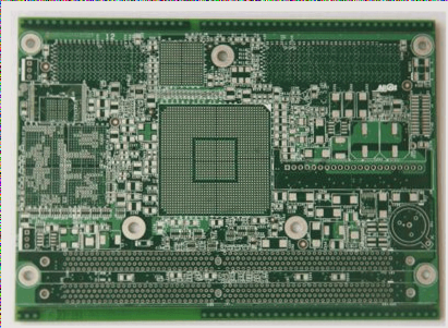
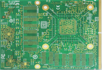
From a functional perspective, vias serve two primary purposes: one is to create electrical connections between different layers of the PCB, and the other is to serve as a means of securing or positioning components. In terms of manufacturing processes, vias can be categorized into three main types: **blind vias**, **buried vias**, and **through vias**.
1. **Blind Vias**: These are holes that connect the top and bottom layers of the PCB with one or more inner layers. They have a limited depth, typically not exceeding a specific ratio relative to their diameter. Blind vias are used to connect surface traces to internal traces without penetrating through the entire board.
2. **Buried Vias**: These are vias that exist only within the internal layers of the PCB. They do not extend to the top or bottom surfaces. Buried vias are typically used when there is a need for more complex internal layer interconnections, without affecting the outermost layers of the PCB.
3. **Through Vias**: As the name suggests, through vias pass entirely through the PCB, connecting the top layer to the bottom layer. These vias are the most common type and are widely used for electrical interconnections between different layers. They can also be used for mounting or positioning components.
From a manufacturing standpoint, blind and buried vias are created using a specialized process before the PCB is laminated. This often involves multiple inner layers, which are stacked and interconnected through these vias. On the other hand, through vias are relatively simpler to produce and cost-effective, which is why they are the most commonly used type in PCB designs.
### Via Design Considerations in PCB Layout
When designing a PCB, the choice of via type is a crucial factor for both performance and cost-efficiency. **Through vias**, being simpler to fabricate, are often the default choice unless specific requirements call for blind or buried vias. While blind and buried vias can offer design flexibility by allowing for more complex routing and layer-to-layer connections, they come at a higher cost due to the additional manufacturing steps required.
Thus, unless a design necessitates the use of blind or buried vias, **through vias** are typically preferred for their cost-effectiveness and ease of integration into most PCB designs. As a rule of thumb, unless specified otherwise, vias in most PCB designs are assumed to be through vias.
### Conclusion
Understanding the different types of vias and their respective applications is essential for optimizing PCB design. By carefully selecting the appropriate via type, engineers can balance cost, performance, and design complexity to achieve the best possible outcome in their PCB manufacturing process.
**PCB Via Design: Key Considerations and Impact on High-Speed Circuits**
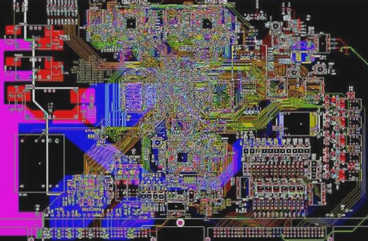
In PCB design, a via consists of two primary components: the central drilled hole and the surrounding pad area. The size of these two parts determines the overall dimensions of the via. In high-speed, high-density PCB designs, minimizing via size is often a priority to maximize routing space. Additionally, smaller vias reduce parasitic capacitance, which is crucial for high-speed signal integrity. However, there are practical limits to how small vias can be made due to manufacturing constraints, such as drilling and plating processes. Below is a detailed analysis of the key factors involved in via design and their implications for PCB performance.
### 1. Via Size and Manufacturing Constraints
In high-speed PCB design, the goal is to minimize via size to optimize board space and reduce parasitic effects. Smaller vias typically result in lower parasitic capacitance, which benefits high-speed circuits by improving signal integrity. However, the size reduction is constrained by the limitations of PCB manufacturing processes, including:
– **Drilling limitations**: As via holes become smaller, the drilling process becomes more challenging. The smaller the hole, the longer it takes to drill, and the more prone it becomes to misalignment. Furthermore, when the hole depth exceeds six times the diameter of the via, uniform copper plating becomes difficult to achieve.
– **Plating challenges**: For example, in a standard 6-layer PCB with a thickness of approximately 50 mil, the minimum via hole diameter achievable by most PCB manufacturers is around 8 mil.
Thus, while smaller vias provide advantages in terms of signal integrity and space savings, there are practical size limits due to process capabilities.
### 2. Parasitic Capacitance of Vias
Vias exhibit parasitic capacitance to the ground, which can affect the performance of high-speed circuits. The capacitance is influenced by the via’s physical dimensions, the PCB thickness, and the dielectric constant of the substrate material. The parasitic capacitance ( C ) of a via can be approximated using the following formula:
[
C = frac{1.41 cdot epsilon cdot T cdot D_1}{D_2 – D_1}
]
Where:
– ( epsilon ) is the dielectric constant of the PCB material
– ( T ) is the PCB thickness
– ( D_1 ) is the via pad diameter
– ( D_2 ) is the isolation hole diameter on the ground layer
For example, for a 50 mil thick PCB with a via that has an inner diameter of 10 mil and a pad diameter of 20 mil, and a ground isolation hole 32 mil from the pad, the parasitic capacitance can be approximated as:
[
C = frac{1.41 times 4.4 times 0.050 times 0.020}{0.032 – 0.020} = 0.517 , text{pF}
]
This capacitance contributes to a rise time delay, which can be calculated as:
[
T_{10-90} = 2.2 cdot C cdot left( frac{Z_0}{2} right) = 2.2 times 0.517 times left( frac{55}{2} right) = 31.28 , text{ps}
]
While this delay may not be significant for a single via, it can accumulate when multiple vias are used in the signal path, especially in high-speed designs with multiple layer transitions.
### 3. Parasitic Inductance of Vias
In addition to capacitance, vias also introduce parasitic inductance, which can have a more detrimental effect on high-speed circuits than capacitance. Parasitic inductance increases the impedance of the via, which can weaken the effectiveness of bypass capacitors and degrade the overall power distribution network.
The inductance ( L ) of a via can be approximated by the following formula:
[
L = 5.08 cdot h left( ln left( frac{4h}{d} right) + 1 right)
]
Where:
– ( h ) is the length of the via
– ( d ) is the diameter of the via hole
For the same via example (inner diameter of 10 mil, pad diameter of 20 mil, and via length 50 mil), the parasitic inductance is calculated as:
[
L = 5.08 times 0.050 times left( ln left( frac{4 times 0.050}{0.010} right) + 1 right) = 1.015 , text{nH}
]
For a signal rise time of 1 ns, the equivalent impedance of the via is:
[
X_L = frac{pi cdot L}{T_{10-90}} = 3.19 , Omega
]
Such impedance can no longer be ignored in high-frequency designs, especially when bypass capacitors are involved, as they may need to traverse multiple vias, compounding the inductance effect.
### 4. Via Design Recommendations for High-Speed PCBs
Given the parasitic effects of vias, careful consideration must be given to via design in high-speed PCBs. The following best practices can help mitigate these issues:
– **Optimize via size for cost and signal integrity**: For 6-10 layer memory module PCBs, using 10/20 mil (drilled/pad) vias is a good balance between cost and performance. For high-density designs, 8/18 mil vias may be considered. For power or ground vias, larger vias should be used to minimize impedance.
– **Reduce PCB thickness**: Thinner PCBs help reduce both parasitic capacitance and inductance, improving overall signal integrity.
– **Minimize via usage**: Avoid unnecessary vias by keeping signal traces on a single layer whenever possible. The fewer the vias, the less parasitic inductance and capacitance.
– **Optimize via placement**: Place power and ground vias near their respective pins to minimize lead length and reduce inductance. Also, use thicker traces for power and ground to reduce impedance.
– **Use grounded vias**: To provide a low-inductance path, place grounded vias near signal vias to form a more efficient return current path. In cases of very high via density, consider reducing or removing pads from certain layers to avoid disrupting the copper layer continuity.
By considering these factors, designers can better manage the parasitic effects of vias in high-speed PCB designs, ensuring both signal integrity and performance.