What is a Via-in-Pad?
As electronic products continue to evolve towards greater miniaturization, multifunctionality, and high integration, PCBs must accommodate higher routing densities. To address this challenge, the via-in-pad design is commonly employed. This design involves placing a via directly beneath the surface-mount component pad, rather than routing the trace around it. The via connects the component pad on the top layer to the internal layers of the PCB.
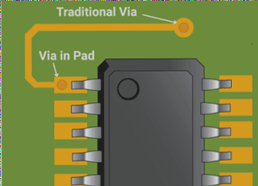
Figure 1: Via-in-Pad
Via-in-Pad Filling
In the via-in-pad process, the vias are typically filled with a non-conductive epoxy, capped, and then plated over to prevent short circuits or incomplete soldering due to tin leakage. This method ensures that the vias are fully filled, reducing the risk of voids and enhancing plating consistency. It is important to note that this process differs from “via tenting,” where the via is covered with a solder mask to prevent solder from flowing into it during assembly.
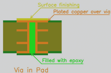
Figure 2: Via-in-Pad Filling
Designing for Via-in-Pad
To effectively design a via-in-pad on a PCB, there are four critical factors to consider. These include selecting the appropriate via size to avoid excessive resistance or capacitance, determining the optimal via placement to minimize signal noise and reflection, ensuring the annular ring size is suitable for maintaining the via’s electrical and thermal properties, and designing the solder mask to prevent solder wicking into the via, which can result in issues like solder voids or solder balls.
When to Use Via-in-Pad in Design?
Is via-in-pad design suitable for every PCB layout? When incorporating a via-in-pad in your design, it is essential to assess whether the following conditions apply to your specific requirements:
Increased Density
When you need to pack a large number of components and traces into a small area, the via-in-pad design can help conserve PCB space by reducing the number of surface-mounted vias.
Improved Thermal Performance
Via-in-pad design can enhance heat dissipation from heat-sensitive components, such as power devices, by providing a direct thermal path to a copper plane.
Improved Electrical Performance
For circuits that require enhanced electrical performance, via-in-pad provides a low-impedance connection between the component and the PCB’s inner layers, improving signal integrity.
High-Frequency Applications
In high-frequency applications, via-in-pad is particularly beneficial for controlling impedance and improving signal integrity.
However, via-in-pad designs also have some potential drawbacks, including increased manufacturing complexity, higher costs, and potential thermal stress on components. Ultimately, the decision to use via-in-pad should be based on the specific requirements and constraints of your design.
If you have any questions about PCBs or PCBA, please contact us at info@wellcircuits.com

