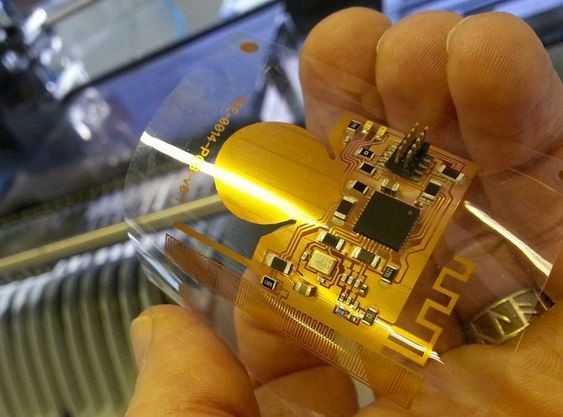
1. Because of their small size and increasing demand, there are currently few standardized printed circuit board (PCB) specifications tailored for the burgeoning wearable Internet of Things (IoT) market. In the absence of these standards, we must draw upon the insights and manufacturing acumen gleaned from board-level development to tackle the unique challenges that lie ahead.
2. Three pivotal areas merit particular attention: PCB base material, RF/microwave design, and RF transmission circuits.
3. PCB Base Material:
4. PCBs typically comprise layers constructed from various materials such as fiber-reinforced epoxy (FR4), polyimide, Rogers material, or other laminates. The insulating material interposed between these layers is referred to as a semi-cured sheet.
5. The exigencies of wearable devices underscore the critical need for heightened reliability. Consequently, PCB designers grapple with the dilemma of selecting between the cost-effective FR4—the predominant material in PCB manufacturing—or opting for more sophisticated and pricier alternatives.
6. Should wearable PCB applications necessitate materials conducive to high speeds and frequencies, FR4 might not emerge as the optimal choice. Notably, the permittivity (Dk) of FR4 stands at 4.5, whereas the more advanced Rogers 4003 series material boasts a Dk of 3.55, with the newer Rogers 4350 series closely trailing at 3.66.

The permitt permittivity of a lamination denotes the ratio of capacitance or energy between a pair of conductors near the lamination to that between a pair of conductors in a vacuum. In high-frequency PCB applications, minimizing loss is paramount. Consequently, Roger 4350, boasting a dielectric coefficient of 3.66, proves more apt for higher frequency applications compared to FR4, which exhibits a dielectric constant of 4.5.
In typical scenarios, the layer count of PCBs utilized in wearables spans from four to eight. An 8-layer PCB should ideally furnish sufficient layers and power supply layers, with wiring layers interleaved between them. This configuration serves to mitigate ripple effects in crosstalk and substantially diminish electromagnetic interference (EMI).
During the circuit board layout design phase, a prevalent scheme involves positioning large formations proximate to the power distribution layer. This approach minimizes ripple effects and substantially mitigates system noise, a critical consideration, particularly within the RF subsystem.
Relative to Rogers materials, FR4 presents a higher dissipation factor (Df), particularly evident at high frequencies. Premium FR4 laminates manifest a Df value of approximately 0.002, markedly superior to standard FR4. Conversely, Rogers laminates boast a Df value of 0.001 or less. The utilization of FR4 materials in high-frequency applications engenders discernible disparities in insertion loss, delineating the power loss from point A to point B when employing FR4, Rogers, or alternative materials.
Manufacturing imperatives dictate a heightened need for impedance control in wearable PCBs, pivotal for ensuring signal integrity. Formerly, the acceptable tolerance for signal-bearing routing stood at ±10%, a threshold inadequate for contemporary high-frequency, high-speed circuits. Presently, the requisite tolerance ranges from ±7%, and in select instances, ±5% or less. Such specifications, alongside other variables, significantly influence the manufacture of wearable PCBs, necessitating stringent impedance controls that limit the pool of capable manufacturers.
The permittivity tolerance of laminations crafted from Rogers UHF material typically adheres to ±2%, with certain products achieving ±1%. Conversely, FR4 laminations exhibit a permittivity tolerance as high as 10%. Consequently, juxtaposing these materials underscores the notably diminished interpolation loss characteristic of Rogers laminates. Indeed, the transmission loss and insertion loss of Rogers laminates register a 50% reduction compared to conventional FR4 materials.
Cost considerations often predominate; however, Rogers offers relatively low-loss, high-frequency lamination capabilities at a competitive price point. For commercial applications, a hybrid PCB configuration amalgamating Rogers with epoxy-based FR4 proves viable, with some layers comprising Rogers material and others featuring FR4.
Frequency considerations primarily govern the selection of Rogers laminates. PCB designers tend to gravitate towards Rogers materials when frequencies exceed 500MHz, particularly in rf/microwave circuits, where precise impedance control is imperative, and heightened performance is requisite.
Rogers materials additionally furnish lower dielectric loss vis-à-vis FR4 materials, boasting a stable dielectric constant across a broad frequency spectrum. Furthermore, Rogers materials exhibit optimal low insertion loss performance essential for high-frequency applications.
The excellent thermal expansion coefficient (CTE) of Rogers 4000 series materials ensures dimensional stability, thereby maintaining circuit board integrity amidst fluctuating frequencies and temperatures. This stability is notably superior to FR4 counterparts, especially during cold, hot, and very hot reflow cycles.
In hybrid lamination scenarios, Rogers and high-performance FR4 can be seamlessly integrated utilizing standard manufacturing techniques, facilitating high manufacturing yields. Notably, Rogers l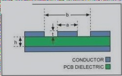
Suspension strip lines are another method of wiring and noise suppression. The line consists of fixed-width wiring in the inner layer and a large ground plane above and below the center conductor. The ground plane is sandwiched between the power layers, providing a very effective grounding effect. This method is preferred for wearable PCB RF signal routing.
Coplanar waveguides provide better isolation near RF lines and lines that need to be run close to each other. The medium consists of a central conductor and a ground plane on either side or below. Both suspension strip lines and coplanar waveguides are the best ways to transmit RF signals, providing better isolation between the signal and the RF routing.
The so-called “through-fence” is recommended for both sides of the coplanar waveguide. This method provides a row of grounding through-holes in each metal ground plane of the central conductor. The mainline running in the middle is fenced on each side, providing a shortcut for the return current to the lower strata. This method can reduce the noise level associated with the high ripple effects of RF signals. The permittivity of 4.5 remains the same as that of the semi-cured sheet FR4 material, while the permittivity of the semi-cured sheet—whether it’s a microstrip line, strip line, or offset stripline—is about 3.8 to 3.9.

1. In some devices that use a ground plane, blind vias may be employed to enhance the decoupling of power capacitance and provide a path to ground.
2. This shunt path to ground shortens the length of through-holes, serving two purposes: it creates a shunt or ground and reduces the transmission distance of devices with smaller footprints, which is critical in RF design.

