After several months of relocation and adjustments, we are excited to announce that our factory has moved to its “new home”! Let us take you on a virtual tour of our state-of-the-art facility.
On the first floor, our team is in full motion. This area is responsible for cutting, drilling, etching, and copper plating. The floor is meticulously clean, free of scale, and equipped with automated copper deposition and plating machinery. The copper plating process, involving 70 minutes of electricity drawing, ensures that the copper thickness in the holes and on the surface significantly exceeds industry standards.
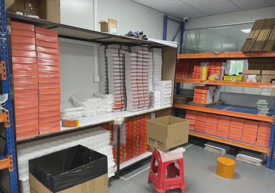
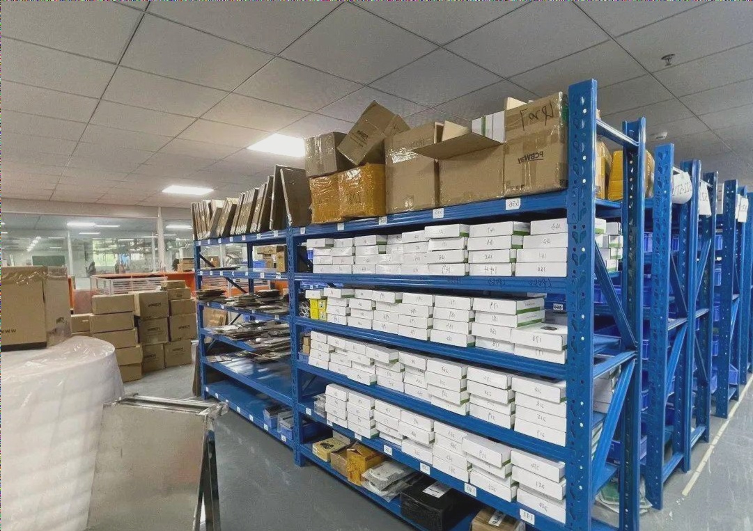
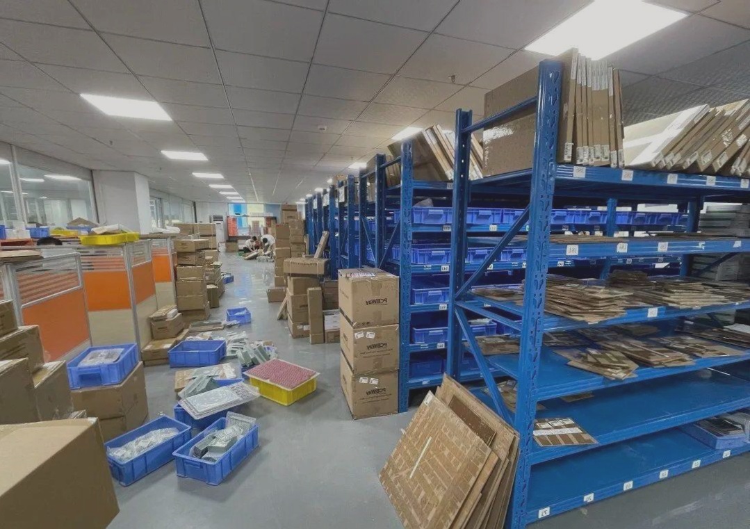
Next, we move to the second floor of Building 33, where our delivery department is located. Here, products are carefully packed into paper boxes, organized in layers for efficient shipping. Our staff is always busy preparing orders, ensuring timely dispatch of customer products.
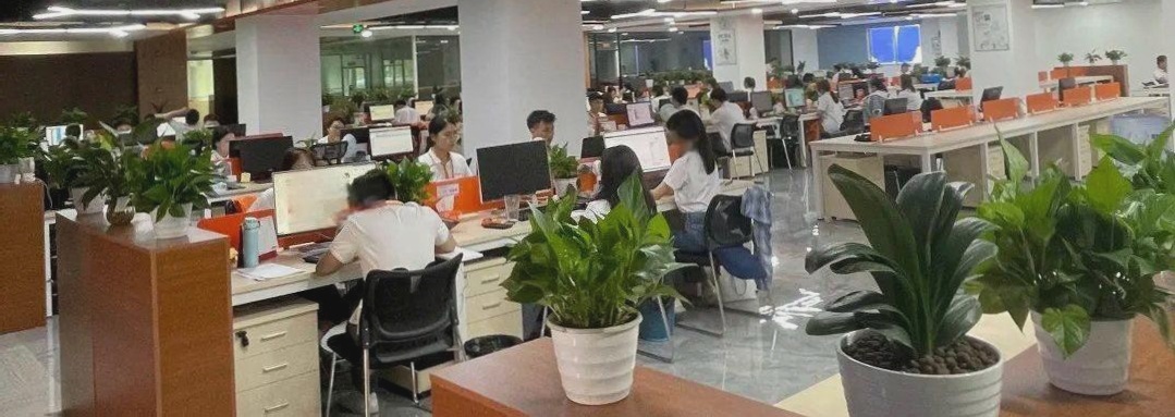
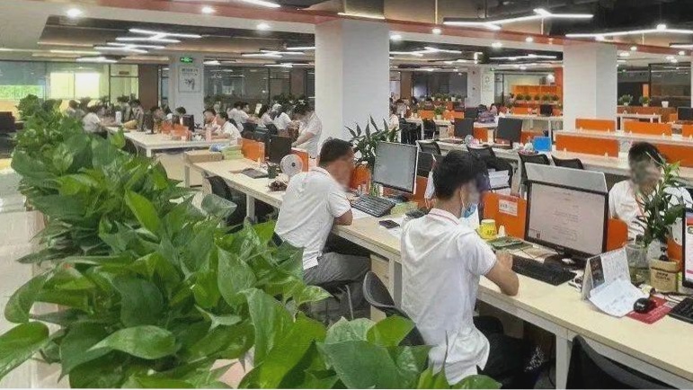
On the third floor, you’ll find our marketing department, where everything is well-organized, from office supplies to various appliances. We work diligently here, ensuring that we serve our customers with the utmost dedication.
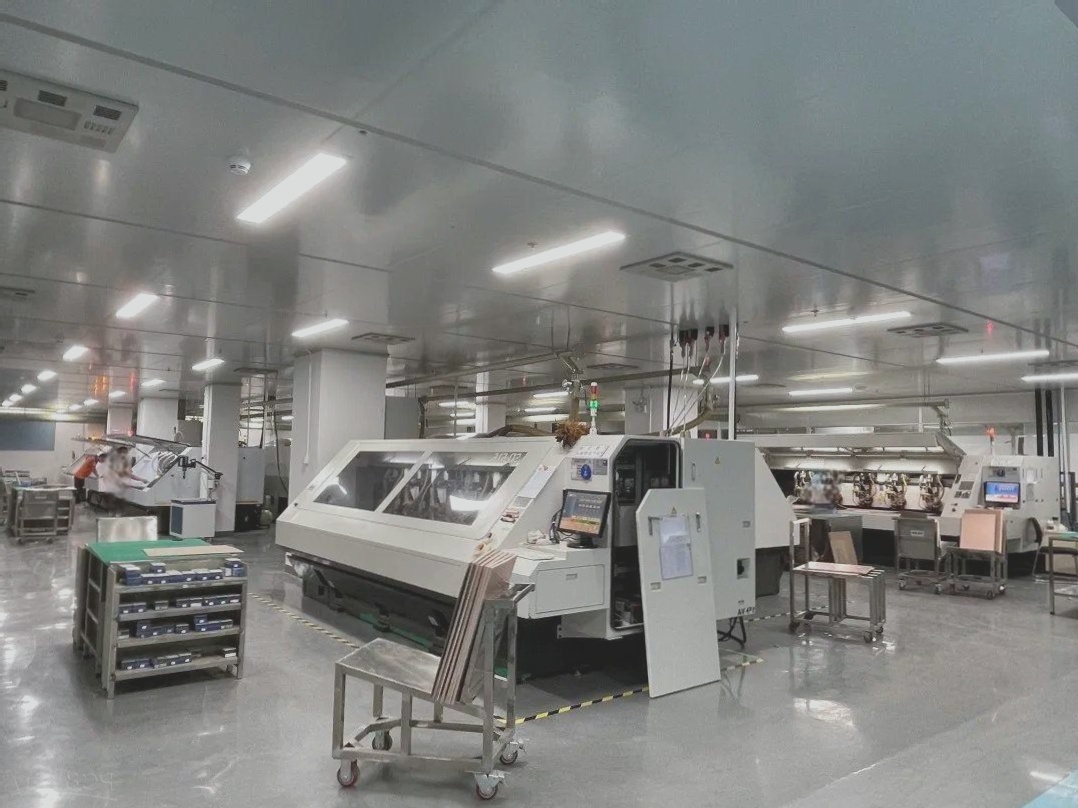
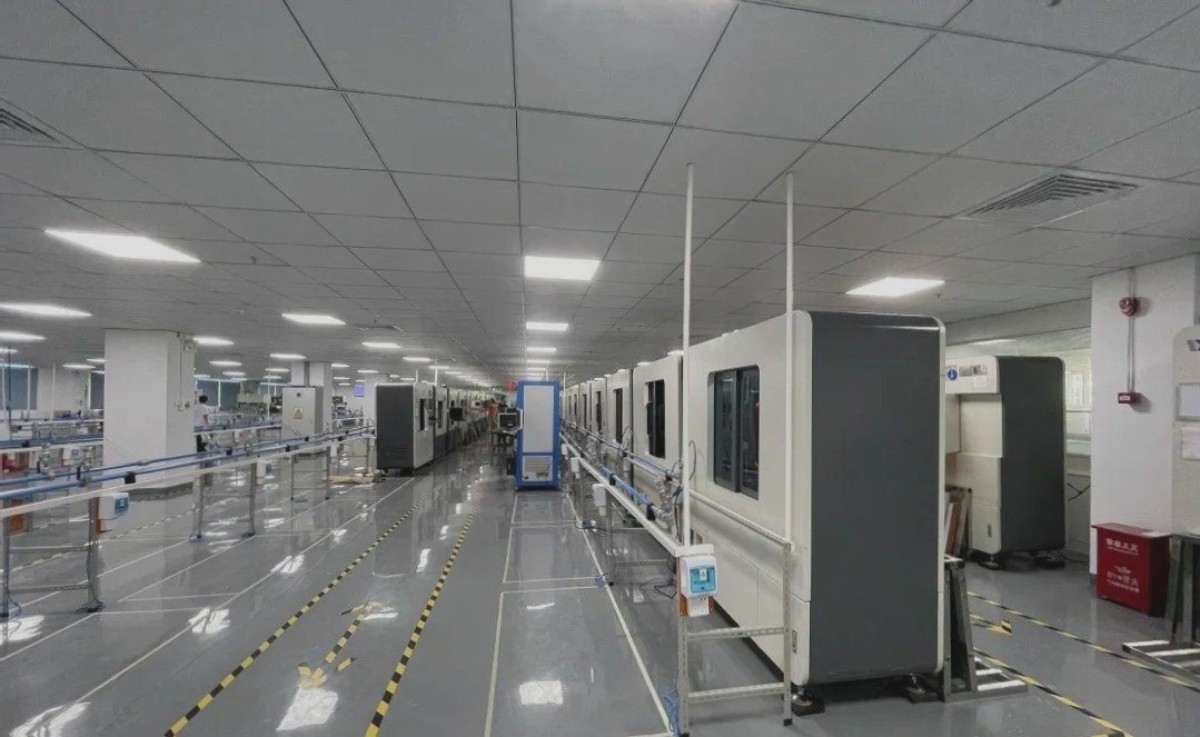
Next, we move upstairs to the core of our operation – the PCB production workshop. This floor houses a variety of large machines arranged in a neat and orderly fashion. The floor and equipment are kept in pristine condition to ensure the highest quality of products. Our team maintains strict cleanliness standards, guaranteeing that every product meets customer expectations.
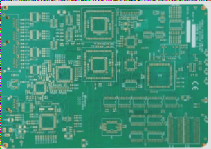
Now, let’s head to Building 32, where the second floor is dedicated to the LDI (Laser Direct Imaging) process. This area utilizes advanced integrated production equipment to precisely control the line width and distance, achieving a minimum of 4 mils. Additionally, the AOI (Automated Optical Inspection) system ensures that any potential quality issues are detected and eliminated.
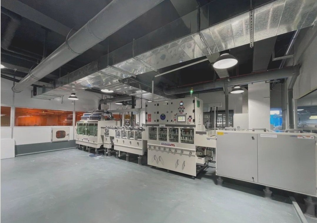
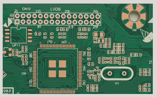
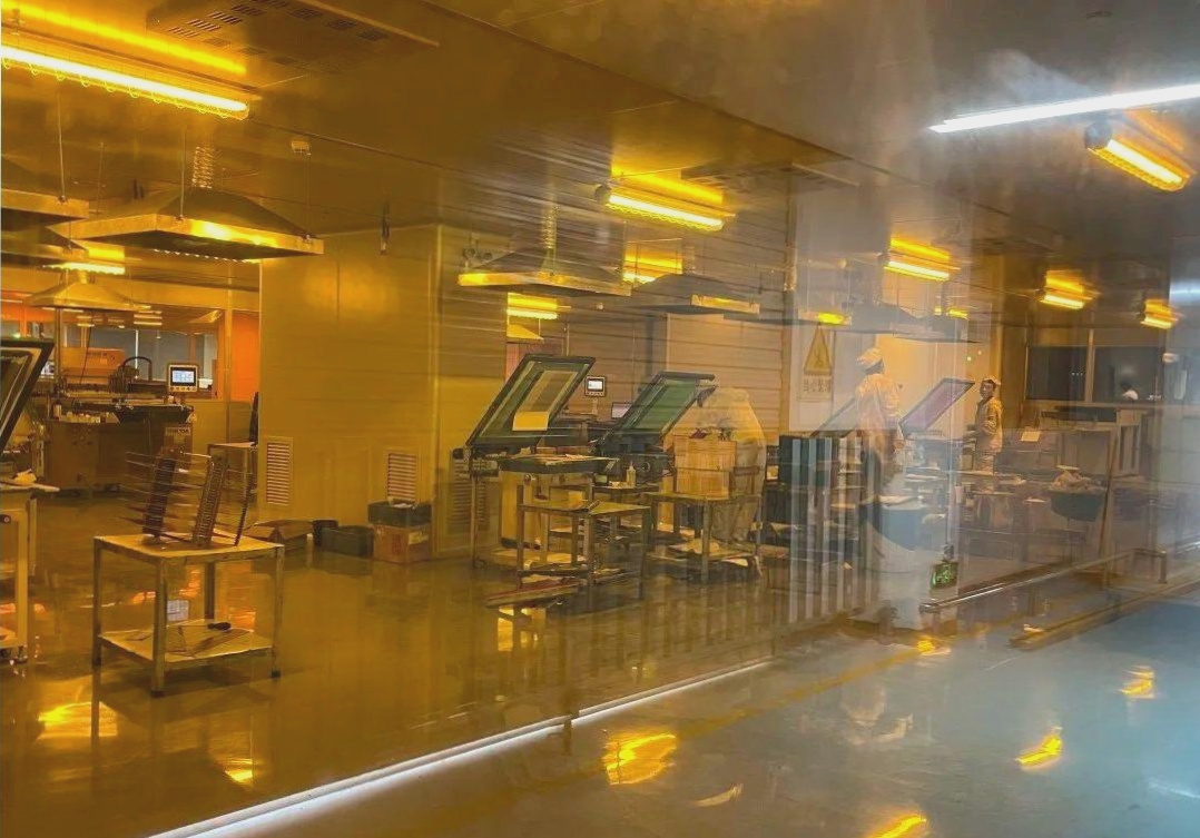
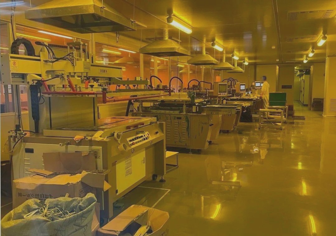
The third floor of Building 32 is our solder mask and character processing workshop. Here, we employ an automated solder mask printing process, followed by multi-zone baking for 80 minutes. This ensures uniform solder mask coverage and adhesion, effectively preventing red copper exposure around the hole rings.
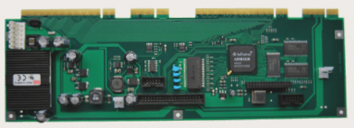
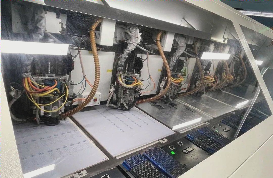
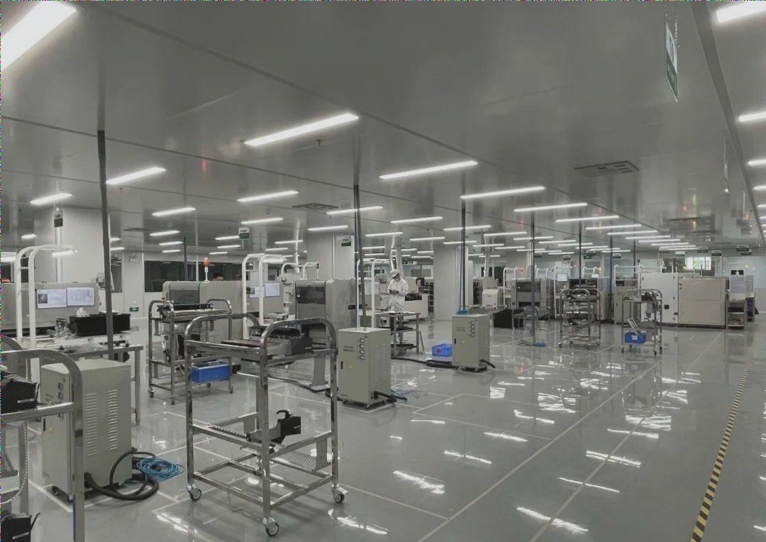
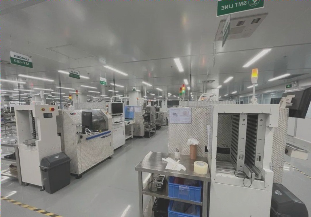
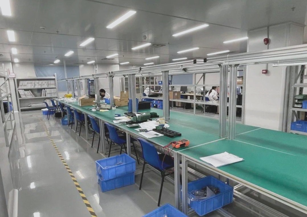
Moving upwards, you’ll find the SMT (Surface-Mount Technology) processing area on the fourth floor, while the fifth floor handles post-soldering processes, including DIP (Dual In-line Package) plug-ins, three-proof coatings, testing, and assembly. Our team is highly trained to perform these tasks with precision and care. In order to maintain product quality, all staff members wear dust caps and shoe covers to prevent any contamination in the workshop.
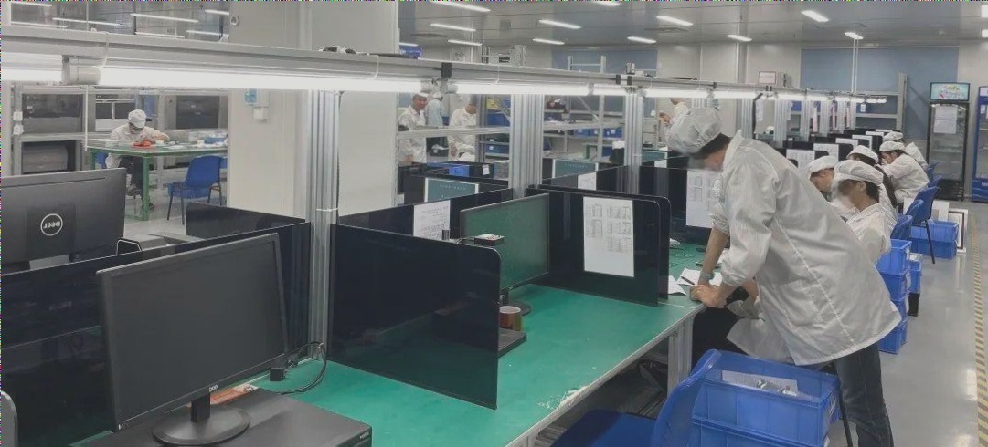
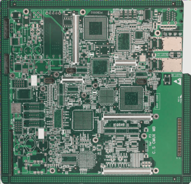
Before shipment, each board undergoes a final inspection on the fifth floor, where flying probe testing or automatic electrical testing is performed. This ensures that any open or short circuits are detected and corrected, guaranteeing that every board shipped to our customers meets the highest quality standards.
Welcome to our “new home”! We would like to express our sincere gratitude to all our customers for their continued support and cooperation throughout our relocation and commissioning process. With our full operations now restored, we are ready to fulfill your orders promptly and efficiently. We invite both new and returning customers to place their orders with us!
If you have any questions about PCBs or PCBA, please feel free to contact us at info@wellcircuits.com.