What is a Bare PCB?
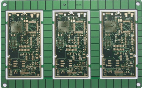
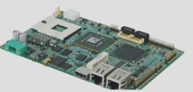
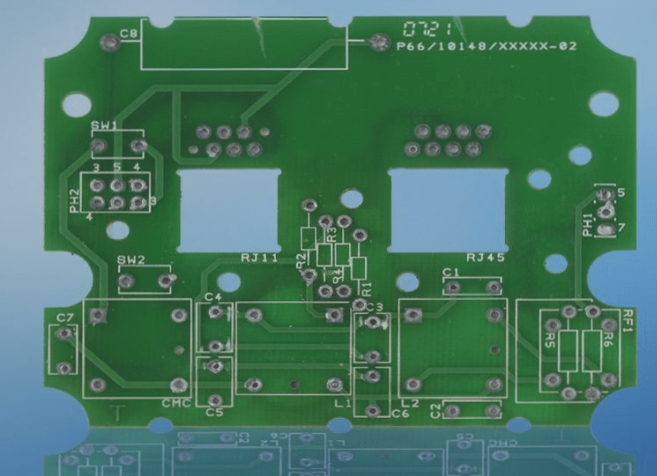
A bare PCB, also known as a blank PCB, is a type of printed circuit board that lacks any electronic components. Typically, these boards consist of a substrate, copper foil traces, solder mask, and silkscreen. However, without components, a bare PCB only provides electrical pathways and does not offer the intended functionality as per its design. It must undergo further processes, such as soldering and assembly, to transform into a fully functional circuit board that serves its intended purpose.

Bare Board Testing
Before assembly, it is essential to verify the integrity of the electrical connections. Many shorts and disconnections may not be detected through simple visual inspection. To assess the electrical connections on a bare board, two common testing methods are used: the flying probe test and the fixture test.
The flying probe test utilizes removable probes with drive devices to contact the test pads and vias on the PCB. This method is highly versatile because it does not require a dedicated fixture and can accommodate a variety of PCB designs.
In contrast, the fixture test, also known as In-Circuit Testing (ICT) or the Bed-of-Nails test, uses a specialized test fixture equipped with numerous probes that match the PCB’s nets precisely. However, if changes are made to the PCB design, the fixture must be reworked, which makes it less flexible for prototype or low-volume production runs.
What is a Zero PCB?
In discussions about bare boards, the term “zero PCB” also comes up, which warrants clarification. A zero PCB, also referred to as a perfboard or DOT PCB, is a type of board not designed for a specific application. Instead, it is a versatile, generic board used for various purposes. Zero PCBs feature small holes arranged in a grid pattern, where each hole is electrically isolated from the others.

Zero PCBs are valuable for testing circuit designs and identifying potential issues. They offer an affordable solution for evaluating circuits before finalizing a design. The term ‘zero’ in this context highlights a key distinction—it indicates that there are no predefined connections, layouts, or functions on the board. Furthermore, ‘zero’ PCBs have additional structural characteristics that set them apart.
Copper Traces or Pads: Zero PCBs have a layer of copper traces or pads on the substrate. These copper elements serve as the conductive paths for soldering electronic components and creating connections. However, the copper traces on zero PCBs are typically not pre-connected, meaning there is no predefined circuit layout. You can build custom circuits by inserting components into the holes and connecting them with wires. This makes the zero PCB function like a breadboard, offering a flexible platform for building custom circuits.
No Solder Mask or Silkscreen: Zero PCBs generally lack a solder mask and silkscreen, which are common features of standard PCBs. The primary purpose of a zero PCB is to provide a blank canvas for users to create and test their own circuits. As a result, they are intentionally kept simple to allow maximum flexibility and experimentation. Users are free to design and solder their circuits directly onto the board without the constraints of a predefined layout or solder mask.


