For those who are electrical engineers or passionate about electronics, they probably do not know the term PCB board. But to understand the basic principle and how to install it in the system of electrical equipment, not everyone knows. So, this article is the answer to the question ” what is a PCB board “?. Along with its characteristics will be shared by us.
1 What is a PCB board?
2 Structure of printed circuit
2.1 Substrate:
2.2 Copper:
2.3 Solder mask:
2.4 Silk Screen:
3 Typical PCB Circuit Types
3.1 Single layer PCB:
3.2 2-layer PCB:
3.3 Multilayer PCB:
3.4 Flexible PCB (flexible PCB):
3.5 Aluminum bottom PCB (rigid):
3.6 Flexible-hard PCB:
3.7 PCB board materials:
4 Conclusion
What is PCB board?
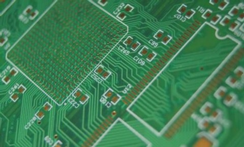
PCB is an acronym for the English phrase Printed Circuit Board. This is a printed circuit board consisting of many layers and is not capable of conducting electricity. The components are connected together on a circuit board and it also has a rack underneath. In the absence of this printed circuit, the components are connected by a type of wire. It increases complexity as well as low reliability. Therefore, it is not possible to create a large circuit board.
Printed circuit construction
An electronic circuit board PCB is composed of many conductive materials. Insulators arranged properly together will form a small circuit board. The materials that make up the PCB board include a substrate, copper, solder mask, and silk screen. To learn more about its structure, we will look at each of these conductive materials in detail.
Substrate:
Made from FR4 glass, it will ensure insulation, sturdy and compact. In terms of size, depending on the location and installation part, there are different sizes. The typical size of printed circuit boards is 1.6 mm thick, which is equivalent to 0.063 inches.
Structure of the PCB board
In addition, some printed circuits have special functions, the substrates are made of more expensive materials such as aluminum, polymers, or RO4350B.
Copper:
This is the second layer of material, a thin copper layer that conducts electricity. Usually copper will have many different layers depending on the application and design requirements. In fact, it can have 1 layer, 2 layers, 3 layers, 4 layers, etc.
Copper is a conductive layer
The thickness of the copper layer is variable and is determined using the mass/area parameter, in oz. According to the estimate as follows:
Weight: 1 oz = 28.35 grams . The specific gravity of copper: 8.9 g/cm3
Length: 1ft = 30.48 cm
Area: 1ft = 0.093 m2
Work out: 1 oz = 1.37 mil
For high-capacity electronic circuit boards, a thickness of 2-3 oz or even more must be used.
Solder mask:
Just above the copper is the solder mask. With the feature of this layer covering the entire circuit except for the component feet to be soldered, this new name is used to refer to it. It acts as isolation between the legs of the component to be soldered and the surrounding circuits. Isolation between circuit lines together; vascular antioxidants. Navigate the small-size SMD component into the correct position when soldering.
layer solder mask circuit board pcb
Silk Screen:
As the top layer, is usually white. It is used to represent the value and position of the component or any other symbol that the designer wants to represent.

Typical types of PCB circuits
PCBs are used to make circuits in electronic devices. Here are some common types of PCBs and their basic characteristics:
Single layer PCB:
The most used type of PCB because of its ease of design and fabrication. One side of the PCB is coated with any conductive material, usually copper. A solder coating is applied to protect the PCB against oxidation. Next is the second layer, which is the marking layer for components.
This type of surface connects electronic components such as resistors, capacitors, etc. It is widely used in the production of computers, radios, printers, and electronic hard drives.
2-layer PCB:
Also known as 2-sided PCB, as the name implies, a thin layer of conductive material. For example, the copper layer is located on both the top and bottom sides of the board. This type is flexible and lower cost, used in industry, manufacturing telephones, converters, UPS systems, etc.
Multilayer PCB:
This type of PCB has more than 2 copper conductive layers. The adhesive layer is sandwiched between the insulation layers to ensure that the heat generated will not damage any components. It has a rather complex structure, so it is often used with small circuits. Or in narrow spaces such as satellite systems, medical equipment, GPS technology
Flexible PCB
Called Fex, it uses flexible materials such as polyimide, polyether ether ketone, or transparent conductive polyester film. The board is designed to be folded or twisted, with a complex structure. It contains different layers such as single-sided flex circuits, double-sided flex circuits, and multi-sided flex circuits. It is applied in complex electronic devices, cameras, mobile phones, and LDC converters.
Aluminum bottom PCB (rigid):
Made of solid material, the PCB does not twist. This type of circuit cannot be bent, the life of the rigid PCB is very long. So, rigid PCB is used in many parts of the computer such as RAM, GPU, and CPU.
Flexible-hard PCB:
Is a combination of flexible and rigid PCB, consisting of layers of flexible PCB attached to multiple layers of rigid PCB. It is used in electronic devices such as cameras, phones, computer support software, etc.
Materials for making electronic circuit boards PCB:
The main components are rigid or flexible dielectric plates. It is built using a conductive material such as copper above. Some typical PCB materials such as FR – glass coating material, CEM made from glass epoxy compound, polyimide – plastic compound, and prepreg – glass fiber impregnated with resin,…
What is the application of PCB?
The PCB is capable of providing power, connecting between components, and customizing any specifications according to the user’s requirements.
PCBs are applied on many electronic devices such as digital cameras, televisions, mobile phones, computer parts such as motherboards, graphics cards… or in fields such as industry. automotive, lighting, medical equipment, industrial machinery…
What is PCBA?
PCBA stands for Printed Circuit Board Assembly. The assembly of electronic components on a PCB is called PCBA. This is a setup and assembly process based on a series of modern technologies such as Auto-Assembly technology, Point-to-point technology, AT technology, and SMT technology.
What is FPCB?
FPCB stands for Flexible Printed Circuit Board, which means flexible printed circuit board. This is a kind of printed circuit board made from polyimide or polyester film, which is characterized by high density, light weight, thinness, and good bendability.
FPCB has good folding or bending ability
This circuit board uses a printing method to shape electrical circuits that connect the electronic components on the insulating board. Fabrication of FPCB is one of the important stages in the process of manufacturing electronic printed circuit boards.
Previously, the fabrication of the FPCB would be separated from the circuit diagramming stage. However, now with the computer-aided design and manufacturing system (CAD-CAM), it is possible to ensure the automatic continuity from the circuit diagram design to the assembly without the intervention of the engineers and create products at a much lower cost.
What is the difference between PCB, PCBA, and FPCB?
FPCB is a type of PCB, so here we only compare and distinguish between the two terms PCB and PCBA.
Distinguish the two terms PCB and PCBA
PCB: is a circuit board, made from glass epoxy resin materials and divided into 4, 6, and 8 layers according to the signal number. PCBA: is the plug-in circuit board assembly process and the SMT process to form the complete circuit boards.
Simply put, the processes on the circuit board are completed on the computer PCBA. When bare PCB boards pass through SMT, the whole process of DIP plug-ins is collectively referred to as PCBA.
In terms of installation
PCB: using electrical connections, supporting mechanical components through the use of spacers. The power lines and some other features are engraved on the copper plate. PCBA: is a complete circuit board after gluing all the solder printed on the PCB, then assembled into different components such as resistors, ICs, capacitors and other components. Examples are transformers, depending on the purpose of the installation.
Conclusion
Thus, to have an overview “what is a PCB board “. We have sent you the most basic information about this electronic circuit board. Hopefully, through the article, you will gain a certain understanding of PCB and its applications in daily life.


