
Mastering PCB Design: A Comprehensive Guide
Unveiling the Intricacies of Printed Circuit Boards
Did you know that your mobile phone houses a miniature football field worth of wires? The unsung hero behind this wire organization is the Printed Circuit Board (PCB).
PCBs play a vital role in the realm of electronics, offering structured and organized homes for components through a network of copper wires. With over 100 meters of wiring intricately connecting the dots, PCBs are the backbone of modern technology.
As technology advances, PCB designing has evolved into a skill that demands expertise and precision. Tools like Allegro and Altium have streamlined the design process, but mastering PCB design requires adherence to essential guidelines.
Essential Guidelines for PCB Designing
Determining Design Rules Before Layout
Before diving into PCB design, establishing design rules is paramount. Collaborating with clients to set the groundwork ensures a smooth design process. Conducting pre-design tests, market research, and material selection lays a strong foundation, minimizing errors and optimizing production efficiency.
Strategic Component Placement
Component placement is a critical aspect of PCB design, influencing functionality and efficiency. By prioritizing key components, minimizing net crossings, and strategically positioning integrated circuits and surface mount devices, designers can optimize board layout and performance.
Optimizing PCB Layout for Success
Efficient PCB layout is crucial for seamless functionality. By adhering to industry standards, minimizing net crossings, and strategically placing components, designers can create high-performance PCBs that meet the demands of modern electronics.
Patience is Key in Component Placement
When designing a PCB, patience is crucial when it comes to component placement. It’s essential to experiment with different layouts until you find the one that fits perfectly for your project.
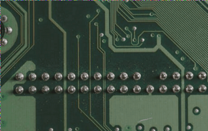
Routing Solutions
After placing components in their correct positions, the next significant step in PCB design is creating a routing solution. Routing involves establishing a network of thin copper wires connecting all components on the board. Proper routing is essential to ensure the functionality and reliability of the PCB.
Power and Ground Planes Placement
Power and ground planes are typically located in the internal layers of a multi-layer PCB. For a two-layer board, it’s recommended to place ground and power planes on alternate layers to optimize performance.
Symmetry in Routing
Creating symmetry in routing is crucial, especially in complex, multi-layered PCBs. Consistent routing patterns help maintain signal integrity and make troubleshooting easier in case of issues.
Optimizing Trace Widths
Using appropriate trace widths based on current requirements is essential for efficient PCB design. Wider traces should be used for high-current segments, while thinner traces are suitable for low-current areas to ensure optimal heat dissipation.
Heat Dissipation through Through Holes
Effective heat dissipation is vital for preventing overheating and ensuring component reliability. Through holes, especially Vias, play a crucial role in dissipating heat across different layers of the PCB.
Component Grouping for Efficiency
Grouping similar components together on the same layers and sides can streamline routing and improve overall PCB efficiency. Grouping components based on their characteristics and thermal ratings can lead to better design outcomes.
Tests and Quality Control
Conducting design rule checks, quality assurance tests, and electrical rule checks are essential steps to ensure the PCB meets industry standards and specifications. These tests help identify and rectify errors before moving into production.
PCB Design Supplier Recommendation
For top-notch PCB design services, consider partnering with WellCircuits PCB Services. Their team of experienced engineers with extensive PCB design expertise can help bring your project to life with precision and quality.
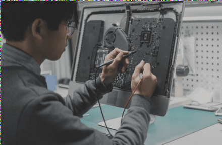
PCB Manufacturing and Design Services
When it comes to PCB manufacturing and designing, you need a one-stop solution that ensures quality and precision every step of the way. Our team of skilled engineers with over a decade of experience meticulously examines PCB designs through DFM, QA, ERC, DRC processes using advanced software like Add, Allegro, Protel, Pads, and Mentor wg before giving the go-ahead for production.
Unmatched Customer Assurance
At our company, customer assurance is our top priority. We pride ourselves on providing unparalleled service that sets us apart as a leader in PCB design and supply. Your raw design is transformed into a top-notch product with our expertise and cutting-edge technology.
The Significance of Printed Circuit Boards
Printed Circuit boards play a vital role in our ever-evolving tech landscape. Innovators constantly strive to enhance PCB performance while reducing its size. Designing and manufacturing PCBs require a unique blend of technical skills and craftsmanship, making it a specialized field.
Key Considerations for PCB Design
Designing a PCB is a complex task that demands attention to detail in component placement, current routing, thermal management, and selecting the right supplier. Making informed decisions at every stage is crucial to ensure the success of your PCB project.
Choosing the Right PCB Design Supplier
Choosing the right PCB design supplier is essential for the success of your product. Look for a supplier that offers a 100% product passing guarantee to ensure the quality and reliability of your PCBs.
