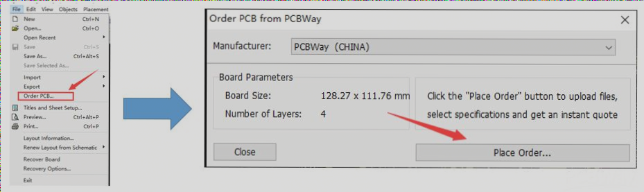
PCB Design Guidelines for Optimal Manufacturing
Line Width and Spacing Considerations
- Minimum line width: 6 mil (0.153 mm)
- Minimum line spacing: 6 mil (0.153 mm)
- Line spacing for paired traces: 0.508 mm (20 mils)
Through-Holes Specifications
- Minimum hole diameter: 0.3 mm (12 mils)
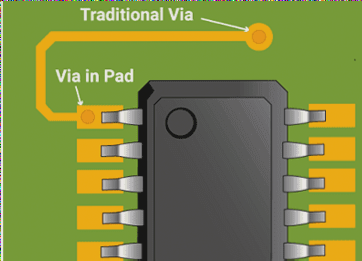
VIA and Pad Guidelines
- Minimum VIA hole aperture: 0.3mm (12 mils)
- Minimum pad size: 6 mil (0.153 mm)
Hole Spacing and Design Considerations
- Hole spacing for VIA holes: at least 6 mil
- Hole spacing for PTH (Plated Through Hole): at least 0.45mm
- Insertion hole (PTH) pad size: at least 0.2mm
Additional Design Tips
- Place PCB shapes on the KEEPOUT or mechanical layer
- Ensure alignment between mechanical and KEEPOUT layers
- Use multiple pads for metalized slots or holes
For detailed PCB design requirements, including considerations for hole spacing, pad sizes, and manufacturing guidelines, follow these expert recommendations to optimize your PCB fabrication process.